Plasma processing system for treating a substrate

a processing system and substrate technology, applied in the direction of coatings, chemical vapor deposition coatings, electric discharge tubes, etc., can solve the problems of ionization and dissociative gas in a common chamber, affecting the operation of the plasma source, and limited control of process chemistry

Active Publication Date: 2008-07-08
TOKYO ELECTRON LTD
View PDF15 Cites 50 Cited by
  • Summary
  • Abstract
  • Description
  • Claims
  • Application Information

AI Technical Summary

Benefits of technology

[0008]Accordingly, one object of an invention of the present application is to reduce or eliminate any or all of the above-described problems.
[0010]Another object of an invention of the present application is to provide a method and system for reducing damage to system components such as a plasma source, and / or to reduce the possibility of damage to a substrate being processed.
[0011]Yet another object of an invention of the present application is to provide a method and system for improving control of process uniformity to a substrate.

Problems solved by technology

First, providing ionization and dissociative gas in a common chamber provides limited control of process chemistry (i.e., control of chemistry dissociation).
Moreover, a common plasma and processing space exposes the plasma source to process gasses that may erode or deposit material on the plasma source thereby affecting the operation of the plasma source.
Similarly, a common gas mixture space may cause substrate damage due to interaction of the substrate with energetic electrons and ions of the plasma.
Still further, the inventor has recognized that the conventional systems are limited to conventional techniques for controlling substrate processing uniformity, such as controlling the temperature of the substrate to compensate for non-uniformity of the plasma and / or process gasses.

Method used


Image

  • Plasma processing system for treating a substrate
  • Plasma processing system for treating a substrate
  • Plasma processing system for treating a substrate

Examples


Embodiment Construction

[0032]In the following description, to facilitate a thorough understanding of the invention and for purposes of explanation and not limitation, specific details are set forth, such as a particular geometry of the plasma processing system and various descriptions of the system components. However, it should be understood that the invention may be practiced with other embodiments that depart from these specific details. Nonetheless, it should be appreciated that, contained within the description are features which, notwithstanding the inventive nature of the general concepts being explained, are also of an inventive nature.

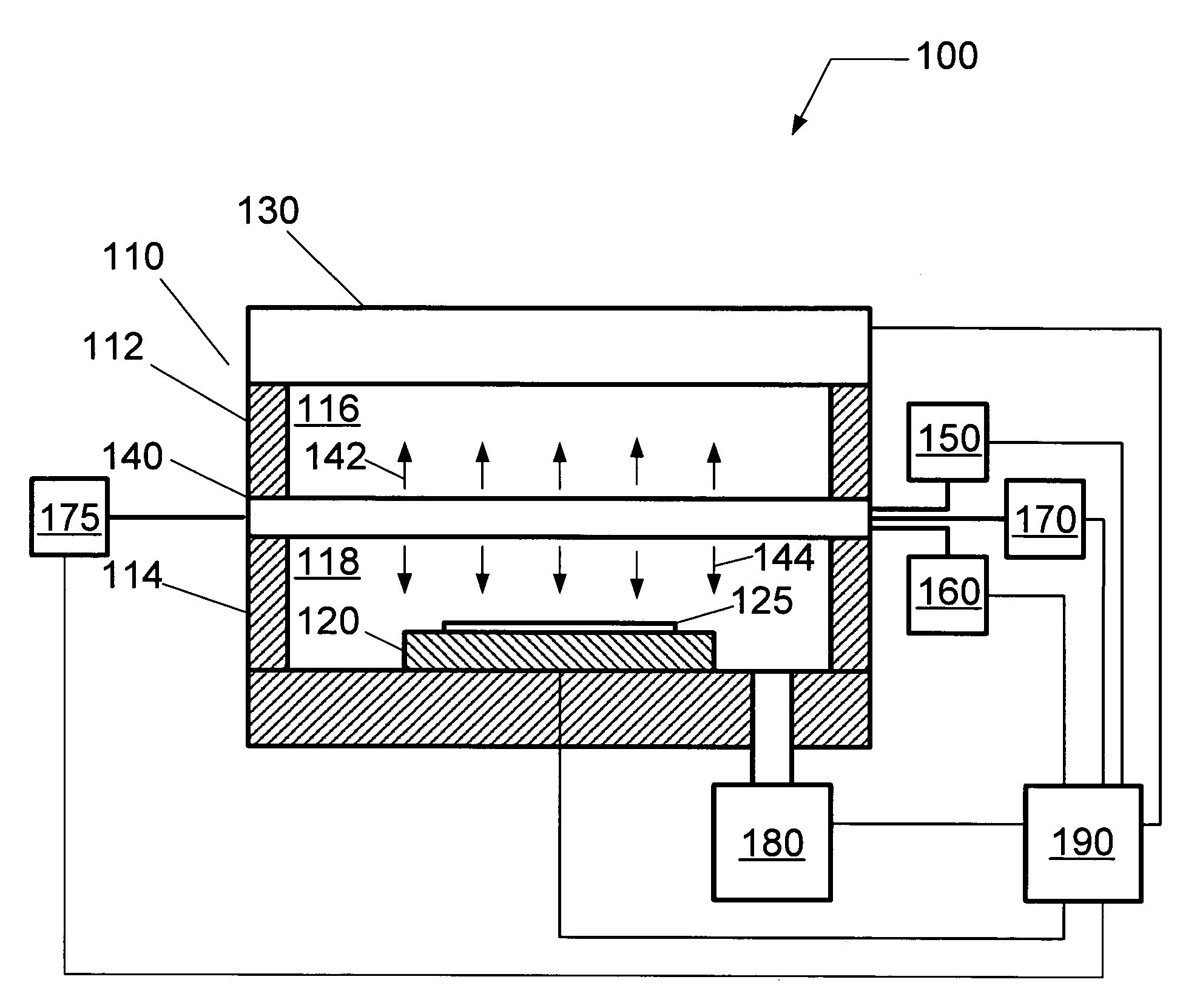
[0033]Referring now to the drawings, wherein like reference numerals designate identical or corresponding parts throughout the several views, FIG. 1 illustrates a plasma processing system 100 according to an embodiment. The plasma processing system 100 comprises a processing chamber 110 having an upper chamber portion 112 (i.e. a first chamber portion) configured to...


PUM

PropertyMeasurementUnit
dielectric constantaaaaaaaaaa
thicknessaaaaaaaaaa
thicknessaaaaaaaaaa

Abstract

A plasma processing system for treating a substrate includes a processing chamber including a first chamber portion configured to receive a first gas for providing a plasma space, and a second chamber portion configured to receive a second gas for providing a process space having process chemistry to treat the substrate. A substrate holder is coupled to the second chamber portion of the processing chamber, and configured to support the substrate proximate the process space, and a plasma source is coupled to the first chamber portion of the processing chamber, and configured to form a plasma in the plasma space. A grid is located between the plasma space and the process space, and configured to permit the diffusion of the plasma between the plasma space and the process space in order to form the process chemistry from the process gas.

Description

CROSS-REFERENCE TO RELATED APPLICATIONS[0001]This application is related to co-pending U.S. patent application Ser. No. 10 / 953,802, entitled “Surface wave plasma processing system and method of using”, filed on even date herewith; co-pending U.S. patent application Ser. No. 10 / 954,086, entitled “Method for treating a substrate”, filed on even date herewith; and co-pending U.S. patent application Ser. No. 10 / 953,791, entitled “Method and system for improving coupling between a surface wave plasma source and a plasma space”, filed on even date herewith. The entire contents of all of those applications are herein incorporated by reference in their entirety.BACKGROUND OF THE INVENTION[0002]1. Field of the Invention[0003]The present invention relates to a plasma processing system and, more particularly, to a plasma processing system configured to control a process chemistry in a space proximate a substrate.[0004]2. Description of Related Art[0005]Typically, during semiconductor processin...

Claims


Application Information

Patent Timeline
Patent Type & Authority Patents(United States)
IPC IPC(8): C23C16/00C23F1/00H01L21/306
CPCH01J37/32082H01J37/32211H01J37/32192H01L21/3065
Inventor CHEN, LEEKAMBARA, HIROMITSUTIAN, CAIZHONGNISHIZUKA, TETSUYANOZAWA, TOSHIHISA
Owner TOKYO ELECTRON LTD
Why Eureka
Try Eureka