

Method and apparatus for controlling the thickness of a selective epitaxial growth layer
- Summary
- Abstract
- Description
- Claims
- Application Information
AI Technical Summary
Problems solved by technology
Method used
Image

Examples
Embodiment Construction
)
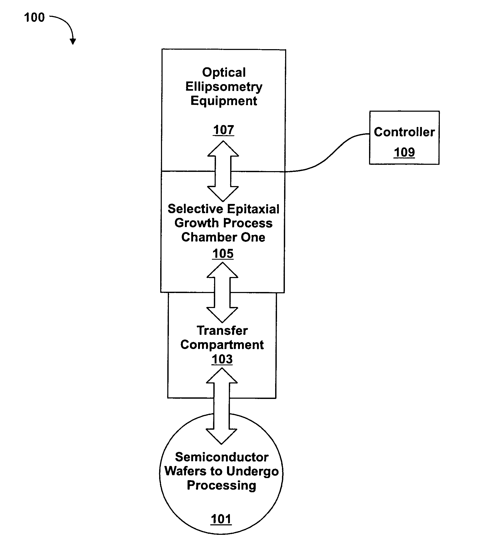
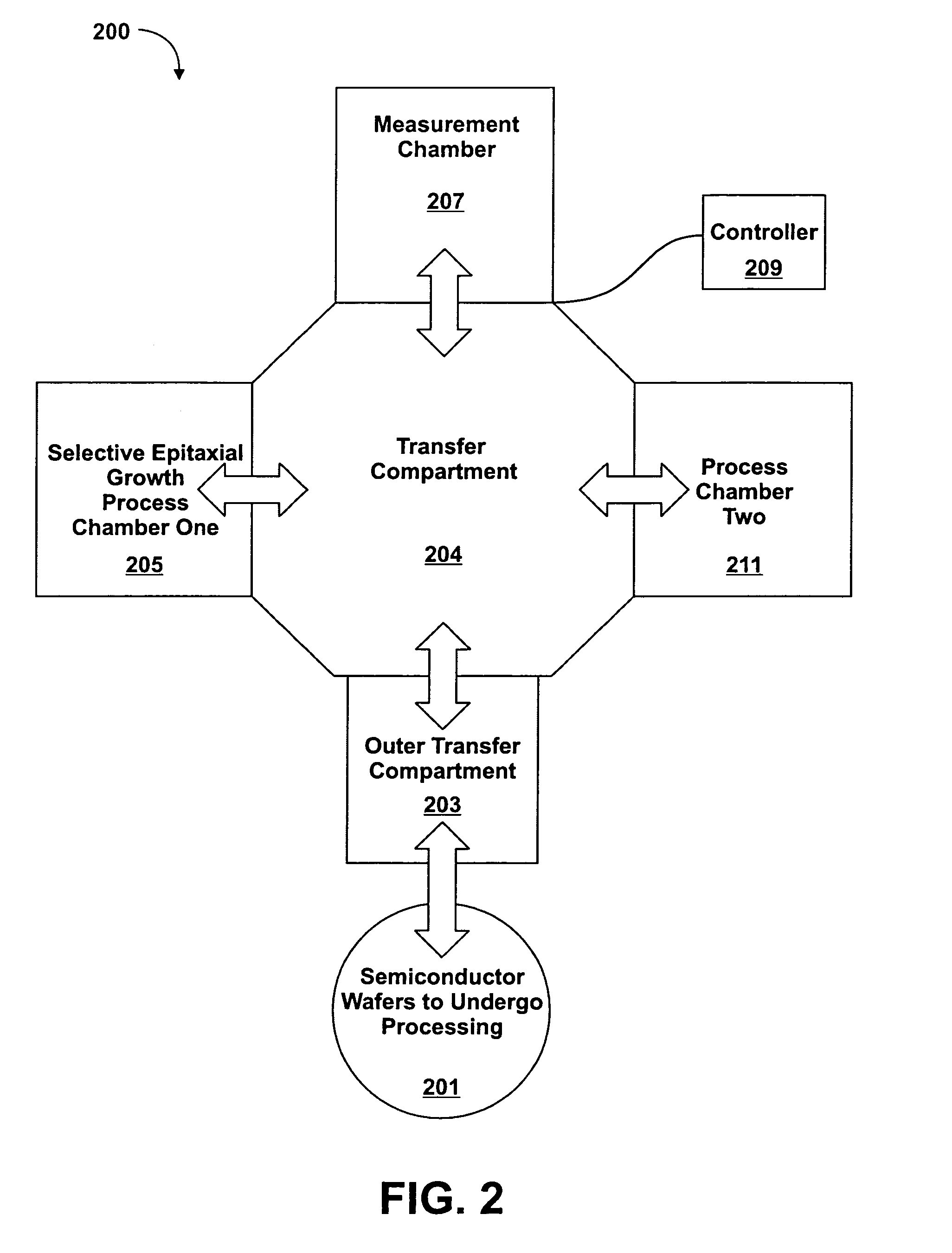
[0013]The present disclosure provides methods and systems for permitting thickness control of the selective epitaxial growth (SEG) layer in a semiconductor manufacturing process, for example raised source / drain (S / D) applications in CMOS technologies. The methods and systems presented provide the capability to measure the thickness of the SEG film in-situ utilizing optical ellipsometry equipment during or after SEG layer growth, prior to removing the wafer from the SEG growth tool or process chamber(s). In the various embodiments, an ellipsometer is integrated into the SEG platform and control software, thus providing automated process control (APC) capability for SEG thickness.
[0014]Because the measurement tool is integrated into the SEG platform, the problem of problem of potential oxidation on the surface of an SEG layer resulting from differences in environmental conditions between the SEG tool and regions outside the SEG process chamber is overcome. The integration of the elli...
PUM
| Property | Measurement | Unit |
|---|---|---|
| Pressure | aaaaa | aaaaa |
| Thickness | aaaaa | aaaaa |
| Pressure | aaaaa | aaaaa |
Abstract
Description
Claims
Application Information