Methods for manufacturing compound-material wafers and for recycling used donor substrates

a technology of donor substrates and compound materials, which is applied in the direction of basic electric elements, electrical equipment, semiconductor devices, etc., can solve the problems of only re-using substrates, deterioration of crystalline quality of donor substrates, and deterioration of crystalline quality of final soi substrates, so as to achieve good quality and reasonable cost

Active Publication Date: 2008-07-29
SOITEC SA
View PDF15 Cites 26 Cited by
  • Summary
  • Abstract
  • Description
  • Claims
  • Application Information

AI Technical Summary

Benefits of technology

[0006]The present invention includes providing methods for manufacturing compound-material wafers and / or methods for recycling or reusing used donor substrates in a manufacturing process for compound-material wafers. These methods allow an increased number of re-uses of the used donor substrate and, at the same time, allow the fabrication of good quality compound-material wafers at reasonable cost.

Problems solved by technology

It appeared, however, that the donor substrate could only be re-used three to four times, because from run to run, the crystalline quality of the donor substrate deteriorated.
As a consequence, the crystalline quality of the final SOI substrate also deteriorated.
Despite this disclosure, however, the number of possible re-uses of donors substrate is still not satisfactory.
In particular, it appears that controlling the initial oxygen content does not prevent crystal defects from appearing in the final SOI layer after multiple reuse.

Method used


Image

  • Methods for manufacturing compound-material wafers and for recycling used donor substrates
  • Methods for manufacturing compound-material wafers and for recycling used donor substrates
  • Methods for manufacturing compound-material wafers and for recycling used donor substrates

Examples


example

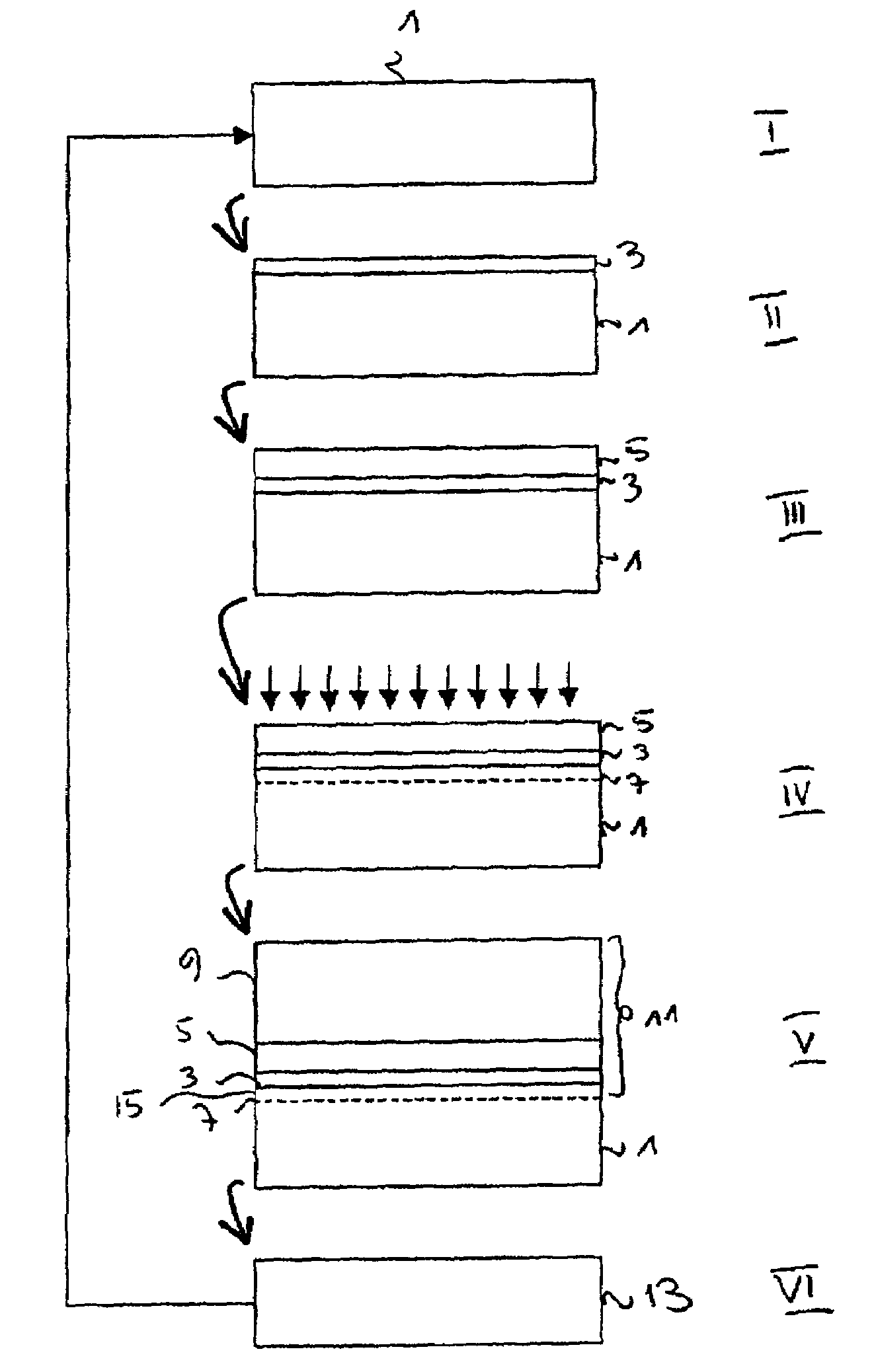
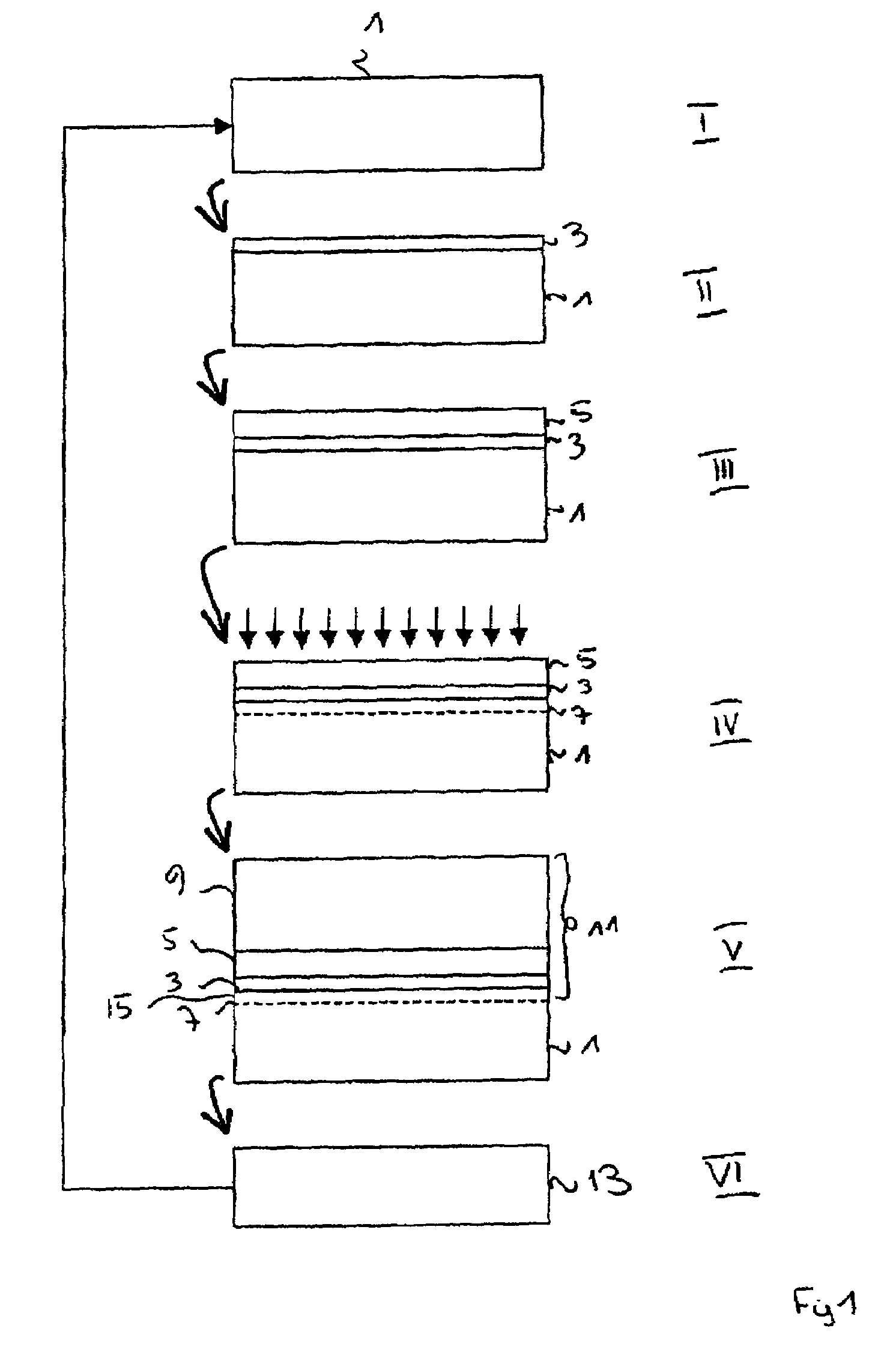
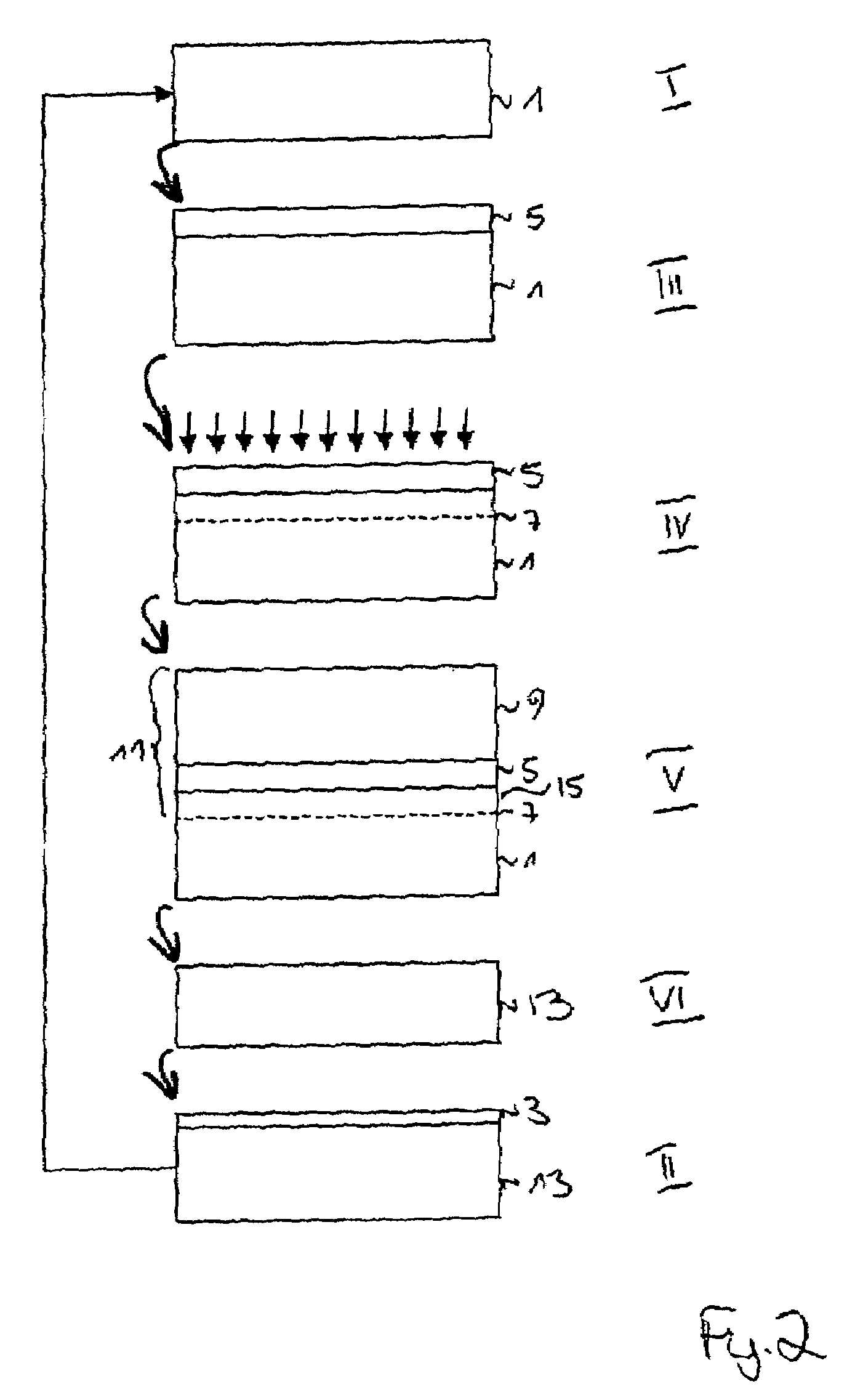
[0046]It has been demonstrated that by carrying out the additional heat treatment step of this invention to reduce oxygen precipitates and / or nuclei, the number of crystalline defaults in the end product, the SOI wafer 11, can be reduced by a factor of at least 6.

[0047]This result has been demonstrated by growing a silicon oxide layer with a thickness of 6000 Å on two silicon wafers. By being 4 times the 1500 Å thickness typical for the isolation layer 5 of a SOI wafer, the growth of this oxide layer was believed to simulate the thermal treatments occurring during four iterations of an SOI fabrication process. For one wafer, no additional heat treatment, e.g., no rapid thermal oxidation, was performed; for the second wafer, the rapid thermal oxidation of this invention was performed. Analysis of the defects found to be present in both wafers demonstrated the above mentioned reduction in crystalline defects.


PUM

PropertyMeasurementUnit
flow rateaaaaaaaaaa
temperatureaaaaaaaaaa

Abstract

This invention provides methods for manufacturing compound-material wafers and methods for recycling donor substrates that results from manufacturing compound-material wafers. The provided methods includes at least one further thermal treatment step configured to at least partially reduce oxygen precipitates and / or nuclei. Reduction of oxygen precipitates and / or nuclei, improves the recycling rate of the donor substrate.

Description

FIELD OF THE INVENTION[0001]The invention relates to methods for manufacturing compound-material wafers and for recycling used donor substrates obtained from the manufacture of compound-material wafers; in particular, this invention related to methods for manufacturing silicon on insulator (SOI) type wafers.BACKGROUND OF THE INVENTION[0002]Use of compound-material wafers, in particular, silicon on insulator (SOI) type wafers, as starting materials in the semiconductor device manufacturing process is becoming more and more important. One way to fabricate such wafers with good crystalline quality at reasonable cost is by transferring a layer from a donor substrate also of good crystalline quality onto a handle substrate. Specifically, donor and handle substrates are bonded, and then the donor substrate is detached at a predetermined splitting area previously formed in the donor substrate. In the SMART-CUT® process, the splitting area is formed by implanting atomic species, in particul...

Claims


Application Information

Patent Timeline
Patent Type & Authority Patents(United States)
IPC IPC(8): H01L21/30
CPCH01L21/76254H01L21/02032H01L27/12
Inventor DELPRAT, DANIELNEYRET, ERICKONONCHUK, OLEGREYNAUD, PATRICKSTINCO, MICHAEL
Owner SOITEC SA
Why Eureka
Try Eureka