Light source apparatus

a technology of light source and light source, which is applied in the direction of solid-state devices, basic electric elements, semiconductor devices, etc., can solve the problems of reducing reliability, reducing luminous efficiency, and high defective rate, so as to prevent light interference, enhance heat radiating effect, and luminous efficiency

Inactive Publication Date: 2008-08-12
LG ELECTRONICS INC
View PDF8 Cites 37 Cited by
  • Summary
  • Abstract
  • Description
  • Claims
  • Application Information

AI Technical Summary

Benefits of technology

[0019]Therefore, an object of the present invention is to provide a light source apparatus and a fabrication method thereof capable of preventing light interference between light emitting devices adjacent to each other by forming a groove in a sub-mount and mounting the light emitting device into the groove, and enhancing heat radiating effect as well as luminous efficiency by collecting light emitted from the side of the light emitting device toward the front of the stem.
[0020]Another object of the present invention is to provide a light source apparatus and a fabrication method thereof capable of increasing operability and improving productivity by bonding the sub-mount to a stem by a flip chip bonding method.

Problems solved by technology

However, since the conventional light source apparatus uses a light emitting device by directly attaching the light emitting device in the form of a chip to a stem, a printed circuit board, a precise wire boding procedure is required and thus the reliability is lowered.
In addition, in case of a light source apparatus in which a light emitting device is attached to a sub-mount and then the sub-mount is attached to a stem, light interference between the light emitting devices adjacent to each other occurs or light emitted from the side of the light emitting device is not collected toward the front of the stem but disperses in all directions, thereby decreasing luminous efficiency.
In addition, since a wire bonding method is used in electrically connecting the sub-mount with the stem in order to supply an external power source, a defective rate is high, process compatibility with other components is difficult because of wires, a long time is taken to process, and product reliability is deteriorated.
Moreover, since heat generated from the light emitting device is transmitted to the stem through the sub-mount, heat generation is delayed to thereby reduce a life span of the light emitting device, the work of the assembly and productivity are deteriorated.

Method used


Image

  • Light source apparatus
  • Light source apparatus
  • Light source apparatus

Examples


first embodiment

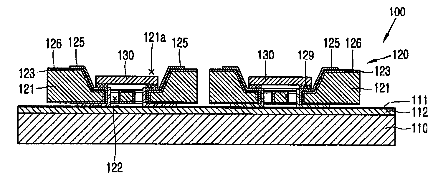
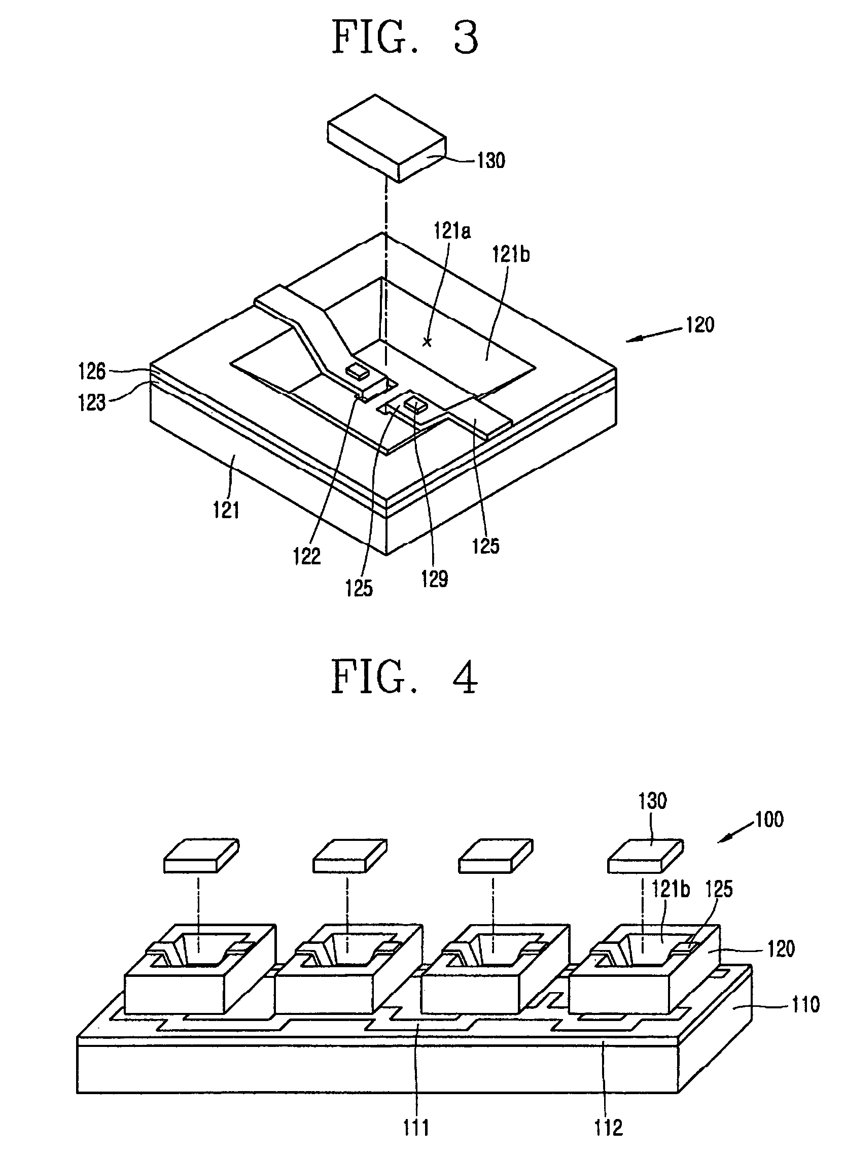
[0045]As shown therein, a light source apparatus 100 in accordance with the present invention includes: a stem 110 having a line pattern electrode 111 at its one surface; a sub-mount 120 provided with a body 121 having a groove 121a at its one surface and through holes 122 inside the groove 121a, a first electrode 125 penetrating the through holes 122 and formed at one surface of the body 121, a second electrode 127 formed at the other side of the body 121 so as to electrically connect with the first electrode 125 and the line pattern electrode 111, and a solder layer 129 formed on the first electrode 125; and a light emitting device 130 inserted into the groove 121a and bonded to the solder layer 129 of the sub-mount 120.

[0046]Preferably, a reflective layer 123 and an insulation layer 126 are sequentially formed on the sub-mount 120 before forming the first electrode 125.

[0047]On the other hand, as for an order of laminating the reflective layer 123 and the insulation layer 125, th...

second embodiment

[0079]Meanwhile, FIGS. 14 to 17 show a sequential process of a method for fabricating a light source apparatus in accordance with the present invention.

[0080]As shown therein, a method for fabricating a light source apparatus in accordance with a second embodiment of the present invention comprises: forming a groove 221a by bulk micro-machining of one surface of a silicon substrate 220′ having an insulation layer 226 at its both sides; forming a first electrode 225 at one surface of the silicon substrate 220′ having the groove 221a and the insulation layer 226; forming through holes 222 by bulk micro-machining of the silicon substrate 220′ at its portion adjacent to the first electrode 225; forming a second electrode 227 at the other surface of the silicon substrate 220′, the second electrode 227 penetrating through the through holes 222 and connecting with the first electrode 225; completing a sub-mount 220 by forming a solder layer 229 on the first electrode 225; bonding a light e...

third embodiment

[0085]Meanwhile, FIGS. 18 to 22 show a sequential process of illustrating a method for fabricating a light source apparatus in accordance with the present invention.

[0086]As shown therein, a method for fabricating a light source apparatus in accordance with the third embodiment of the present invention comprises: forming a groove 321a by removing a part of one surface of a silicon substrate 320′ having an insulation layer 326 at its both surfaces by a bulk micro-machining method; forming through holes 322 by dry-etching a part of the groove 321a; forming a first electrode 325 on one surface of the silicon substrate 320′ by passing through the first electrode 325; forming a second electrode 327 at the other surface of the silicon substrate 320′, the second electrode 327 penetrating through the through holes 322 and connecting with the first electrode 325; completing a sub-mount 320 by forming a solder layer 329 on the first electrode 325; bonding a light emitting device 330 to the so...


PUM


Abstract

A light source apparatus and a fabrication method thereof can prevent light interference between light emitting devices adjacent to each other by forming a groove in a sub-mount and bonding a light emitting device to the groove, enhance heat radiating effect as well as luminous efficiency by collecting light emitted from the side of the light emitting device toward the front of the light source apparatus, reduce the process time and costs and increase reliability by directly connecting the sub-mount to the stem by the first electrode and the second electrode which pass through holes of the sub-mount, and extend a life span of the light emitting device because of the enhanced heat radiating effect.

Description

BACKGROUND OF THE INVENTION[0001]1. Field of the Invention[0002]The present invention relates to a light source apparatus and a fabrication method thereof, and more particularly, to a light source apparatus and a fabrication method thereof capable of not only collecting light emitted from the front of a stem without losing light emitted from each light emitting device but also easily bonding a sub-mount to the stem by forming through holes on the sub-mount.[0003]2. Description of the Background Art[0004]A light emitting device which is currently and actively being used is typically divided into a laser diode (LD) and a light emitting diode (LED).[0005]The LD is being widely used as a light source in the field of optical communication, and has lately been used as an important component in the field of optical media such as a DVD player, a laser disc (LD) player, a mini disc (MD) player, or the like as well as in the filed of a compact disc (CD) player and a compact disc rewritable (C...

Claims


Application Information

Patent Timeline
Patent Type & Authority Patents(United States)
IPC IPC(8): H01L33/00H01L33/48H01L33/64
CPCH01L33/486H01L33/64H01L2224/16H05K1/183H01L2924/12041H05K1/053H01L2924/00014H01L2924/00011H01L2224/0401
Inventor KIM, GEUN-HOSONG, KI-CHANGKIM, SUN-HO
Owner LG ELECTRONICS INC
Why Eureka
Try Eureka