Method and systems for total focus deviation adjustments on maskless lithography systems

a technology of maskless lithography and total focus deviation, applied in the field of lithography, can solve problems such as the deviation of the slm array from a flat plane, and achieve the effect of less stringent optics and reduced total focus deviation

Inactive Publication Date: 2008-08-19
ASML HLDG NV
View PDF42 Cites 5 Cited by
  • Summary
  • Abstract
  • Description
  • Claims
  • Application Information

AI Technical Summary

Benefits of technology

[0015]With the present invention, aberrations such as total focus deviation can be reduced without making high-precision adjustments to lenses in the optical system. Further, correcting aberrations with the SLMs allows a less stringent specification for the optics when the system is built.

Problems solved by technology

This causes the SLM array to deviate from a flat plane.

Method used


Image

  • Method and systems for total focus deviation adjustments on maskless lithography systems
  • Method and systems for total focus deviation adjustments on maskless lithography systems
  • Method and systems for total focus deviation adjustments on maskless lithography systems

Examples


Embodiment Construction

Overview

[0033]While specific configurations and arrangements are discussed, it should be understood that this is done for illustrative purposes only. A person skilled in the pertinent art will recognize that other configurations and arrangements can be used without departing from the spirit and scope of the present invention. It will be apparent to a person skilled in the pertinent art that this invention can also be employed in a variety of other applications.

Maskless Lithography Systems

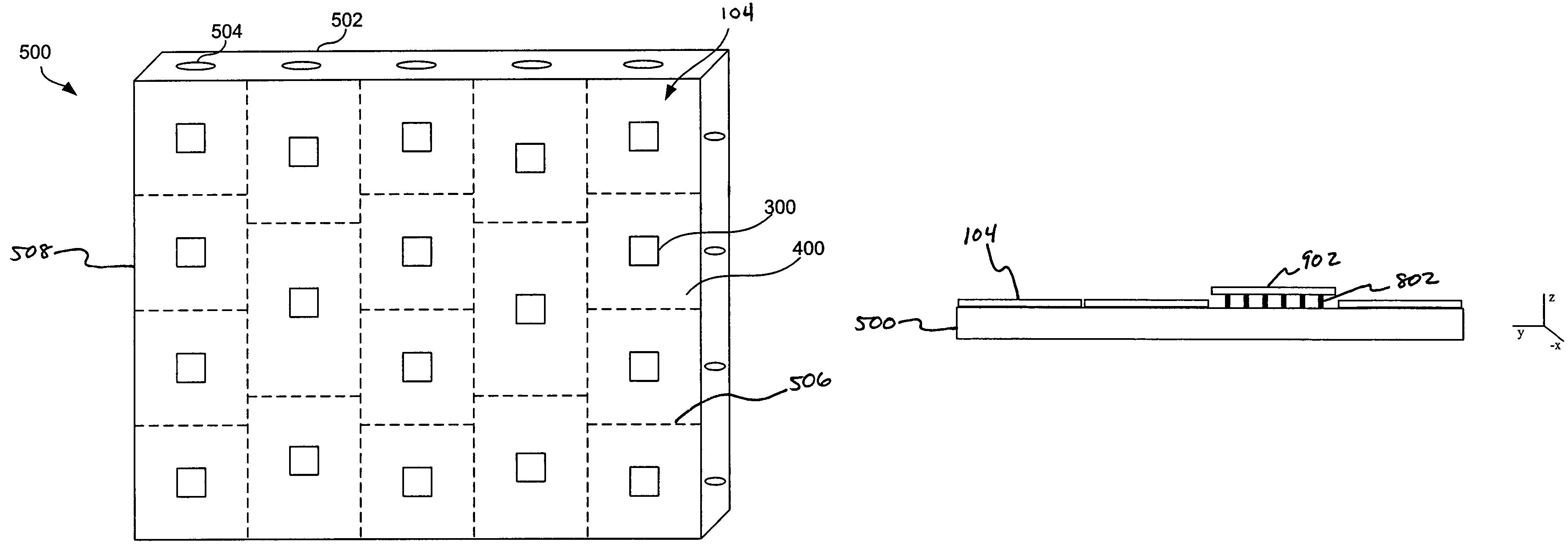
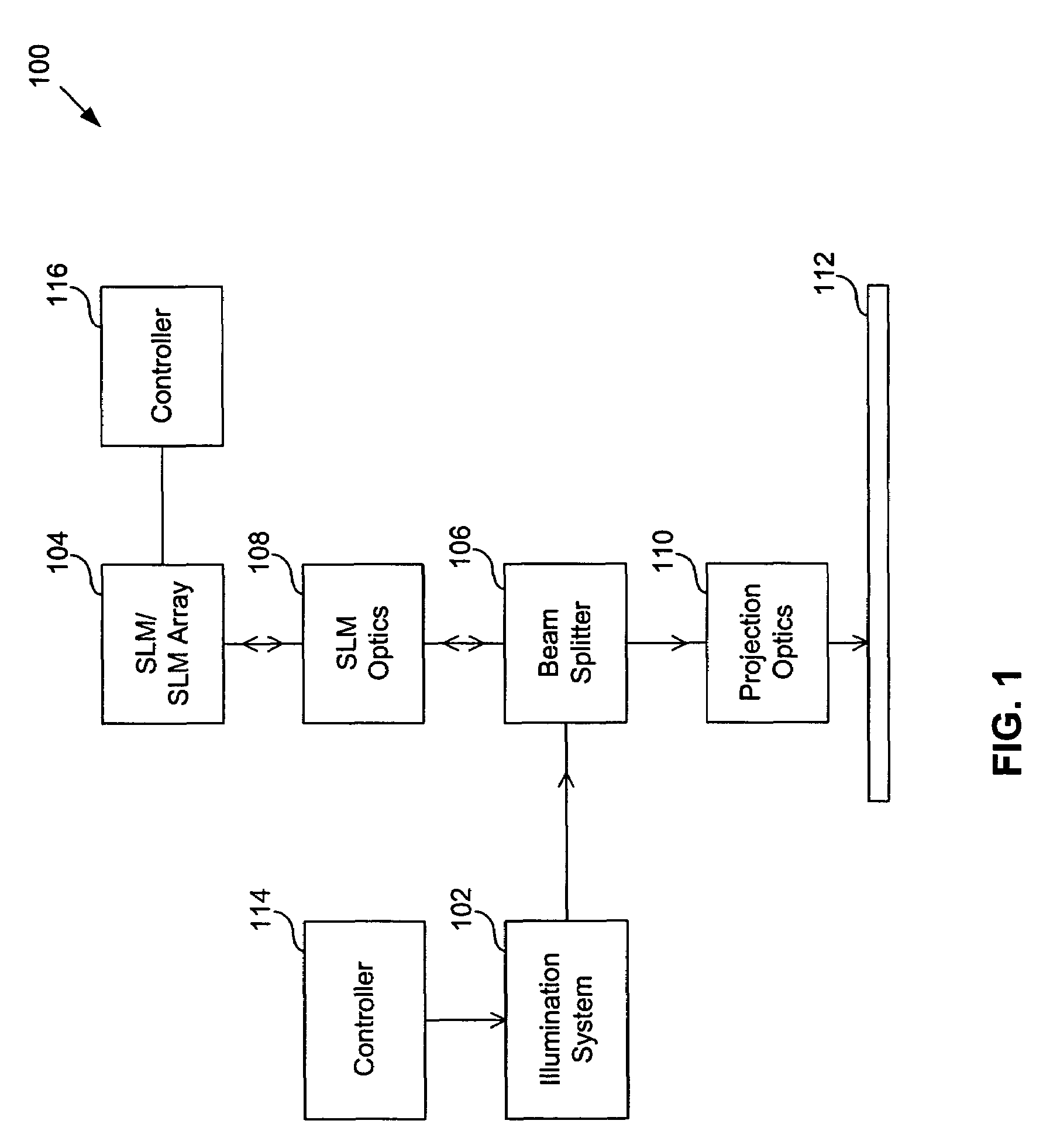
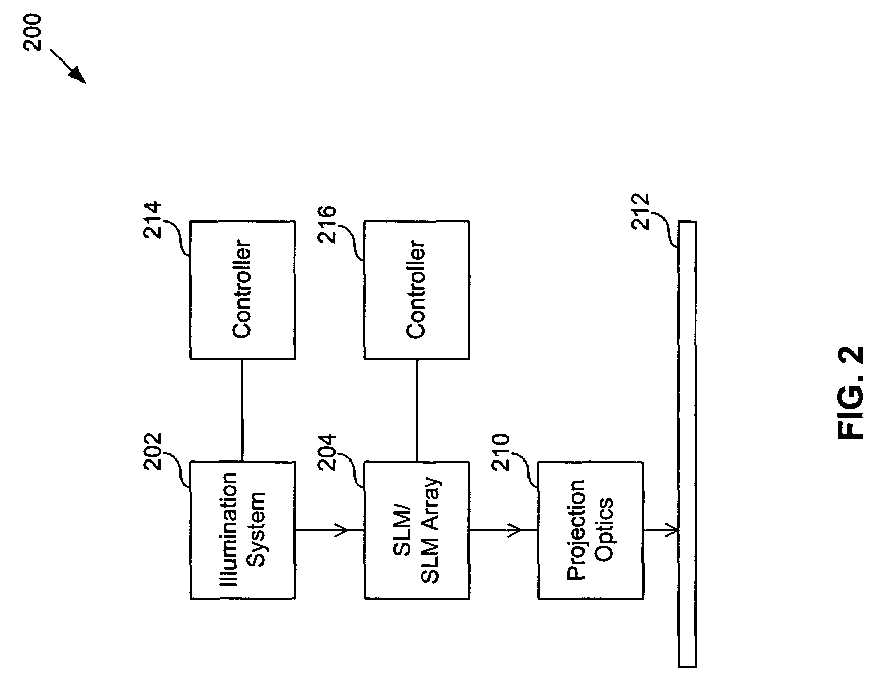
[0034]FIG. 1 shows a maskless lithography system 100 according to an embodiment of the present invention. System 100 includes an illumination system 102 that transmits light to a reflective spatial light modulator (SLM) 104 (e.g., a digital micromirror device (DMD), a reflective liquid crystal display (LCD), or the like) via a beam splitter 106 and SLM optics 108. SLM 104 is used to pattern the light in place of a reticle in traditional lithography systems. Patterned light reflected from SLM 104 is ...


PUM

PropertyMeasurementUnit
angleaaaaaaaaaa
optical aberrationaaaaaaaaaa
conductiveaaaaaaaaaa

Abstract

A method and system for correcting optical aberrations in a maskless lithography system. Adjusters move individual spatial light modulators (SLMs) in an SLM array so that the surface of the SLM array deviates from a flat plane. The deviation compensates for aberrations in the lithography system, such as total focus deviation. In an embodiment, an individual SLM can be tilted, bent, and / or have its elevation changed. Multiple SLMs in the SLM array can move in different ways depending on the compensation to be made. The adjusters can be either actively or passively controlled. The method may be performed only during initial setup of the maskless lithography system, periodically as needed for maintenance of the lithography system, or prior to each exposure in the lithography system.

Description

BACKGROUND OF THE INVENTION[0001]1. Field of the Invention[0002]The present invention is directed generally to lithography. More particularly, the present invention relates to maskless lithography.[0003]2. Related Art[0004]Lithography is a process used to create features on the surface of substrates. Such substrates can include those used in the manufacture of flat panel displays (e.g., liquid crystal displays), circuit boards, various integrated circuits, and the like. A frequently used substrate for such applications is a semiconductor wafer or glass substrate. While this description is written in terms of a semiconductor wafer for illustrative purposes, one skilled in the art would recognize that this description also applies to other types of substrates known to those skilled in the art.[0005]During lithography, a wafer, which is disposed on a wafer stage, is exposed to an image projected onto the surface of the wafer by exposure optics located within a lithography apparatus. Wh...

Claims


Application Information

Patent Timeline
Patent Type & Authority Patents(United States)
IPC IPC(8): G03B27/52G02B26/00G03F7/20
CPCG03F7/70283G03F7/70291G03F7/70783G03F7/707G03F7/703
Inventor KOCHERSPERGER, PETER
Owner ASML HLDG NV
Why Eureka
Try Eureka