Solid-state imaging device and manufacturing method for the same

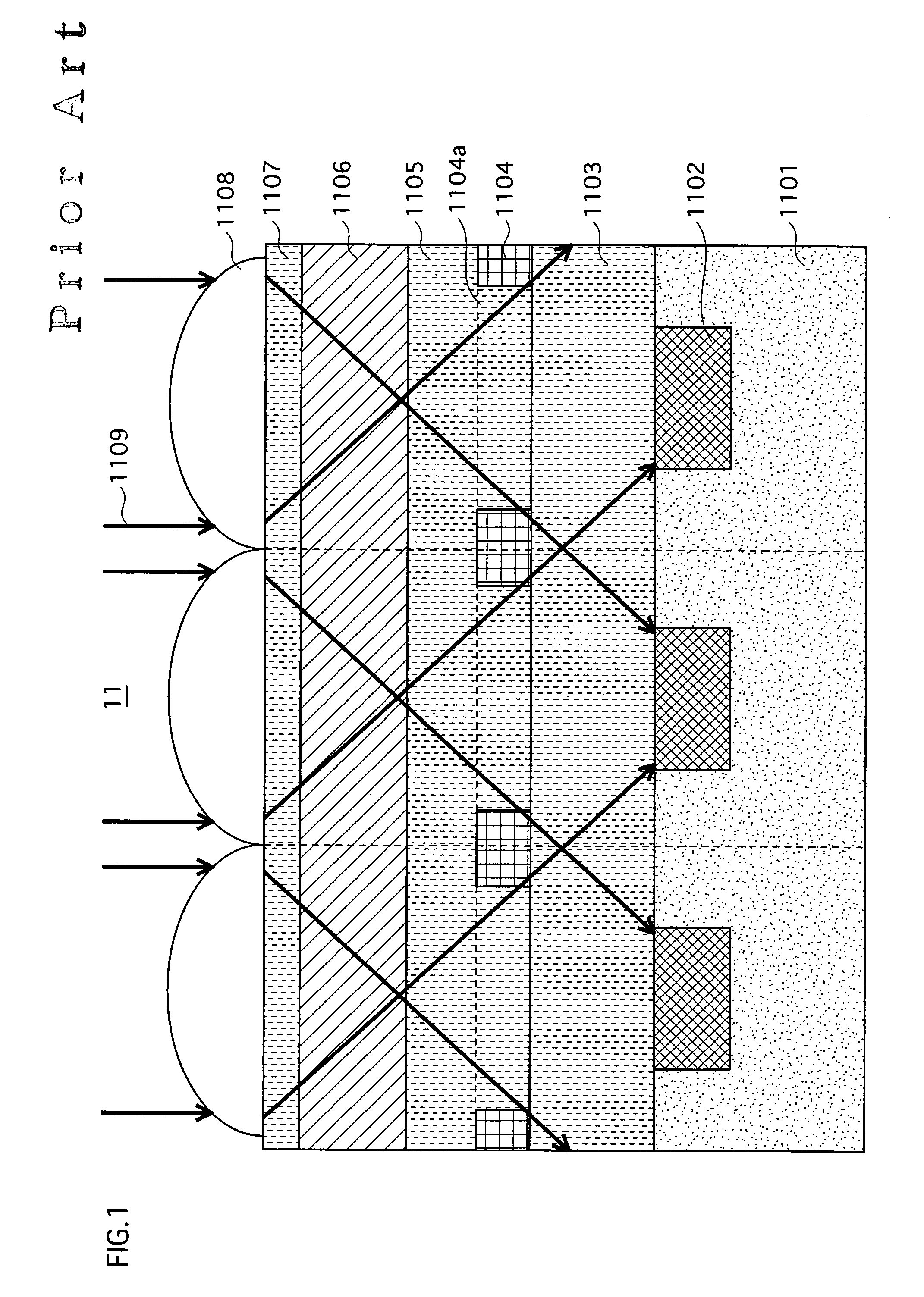
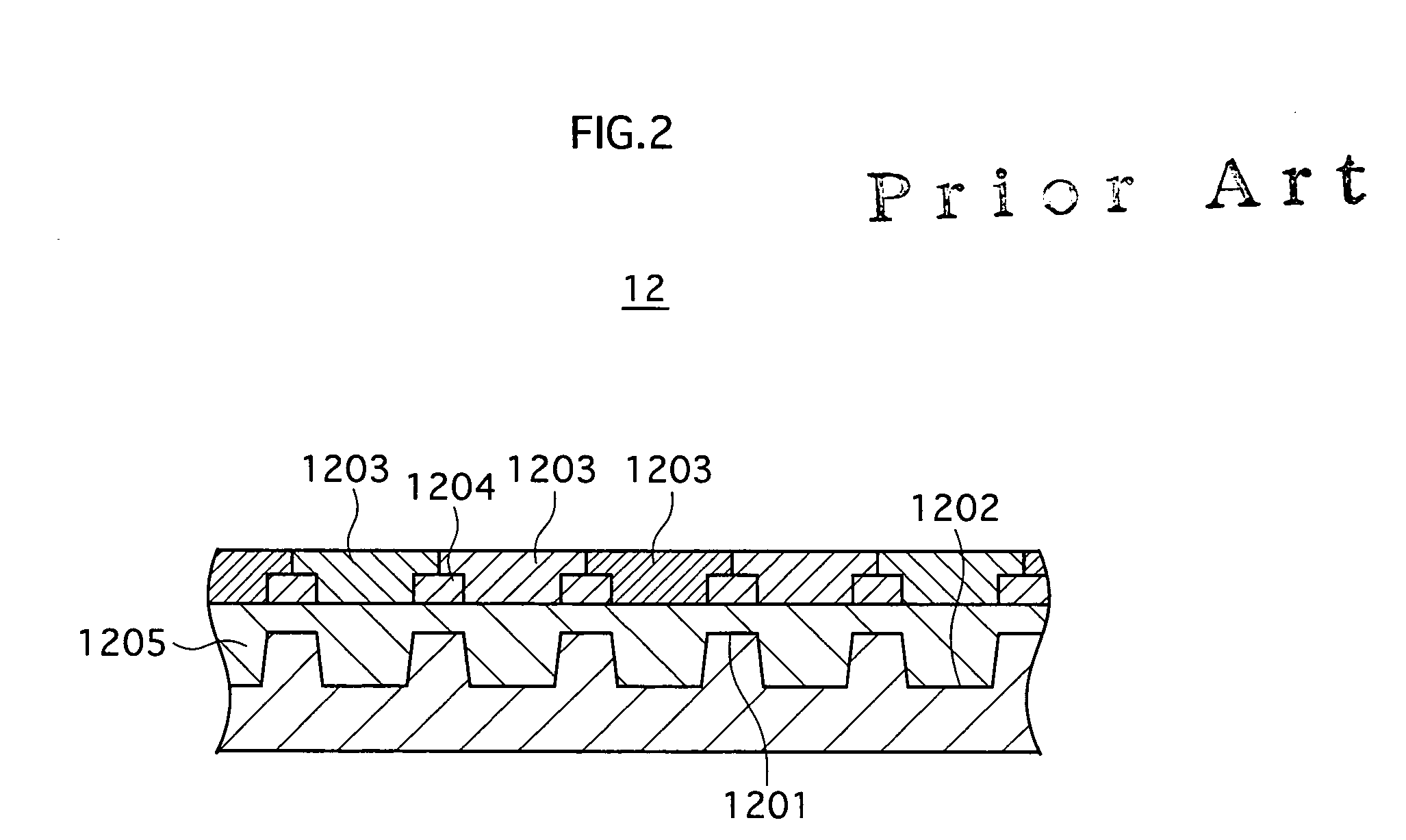
a technology of solid-state imaging and manufacturing methods, which is applied in the direction of optical radiation measurement, instruments, television systems, etc., can solve the problems of reducing sensitivity, limiting this miniaturization, and reducing so as to prevent color mixing and reduce the thickness of solid-state imaging devices

Active Publication Date: 2008-08-26
PANASONIC CORP
View PDF9 Cites 21 Cited by
  • Summary
  • Abstract
  • Description
  • Claims
  • Application Information

AI Technical Summary

Benefits of technology

[0015]It is possible to reduce a thickness of the solid-state imaging device if the color filter composed of inorganic material (hereinafter, “inorganic filter”) is disposed in the aperture of the light shielding film. It is also possible to eliminate color-mixing due to oblique light since the distance between the color filter and the photoelectric converter is reduced, as can the distance between the color filter and a lens which focuses incident light onto the photoelectric converter.
[0030]As mentioned above, the multilayer interference filter is disposed in the aperture of the light shielding film in the present invention, thereby enabling the thickness of the solid-state imaging device to be reduced 2 μm more than conventional technology. Consequently, it is possible to prevent color-mixing due to an increasing number of pixels, etc.

Problems solved by technology

However, there is a limit to this miniaturization since the pigment particles which constitute the color filters 1106 have a particle diameter of 0.1 μm.
For this reason, as the film thicknesses of the color filters 1106 are excessively reduced, the distribution of pigment particles ceases to be uniform, sensitivity reduction and color irregularities occurs, and the color filters become impractical for use.
However, even with this structure it is not possible to prevent color-mixing since the color filters remain thick enough to allow oblique light.

Method used


Image

  • Solid-state imaging device and manufacturing method for the same
  • Solid-state imaging device and manufacturing method for the same
  • Solid-state imaging device and manufacturing method for the same

Examples


embodiment 1

[0046](1) Structure of the Solid-State Imaging Device

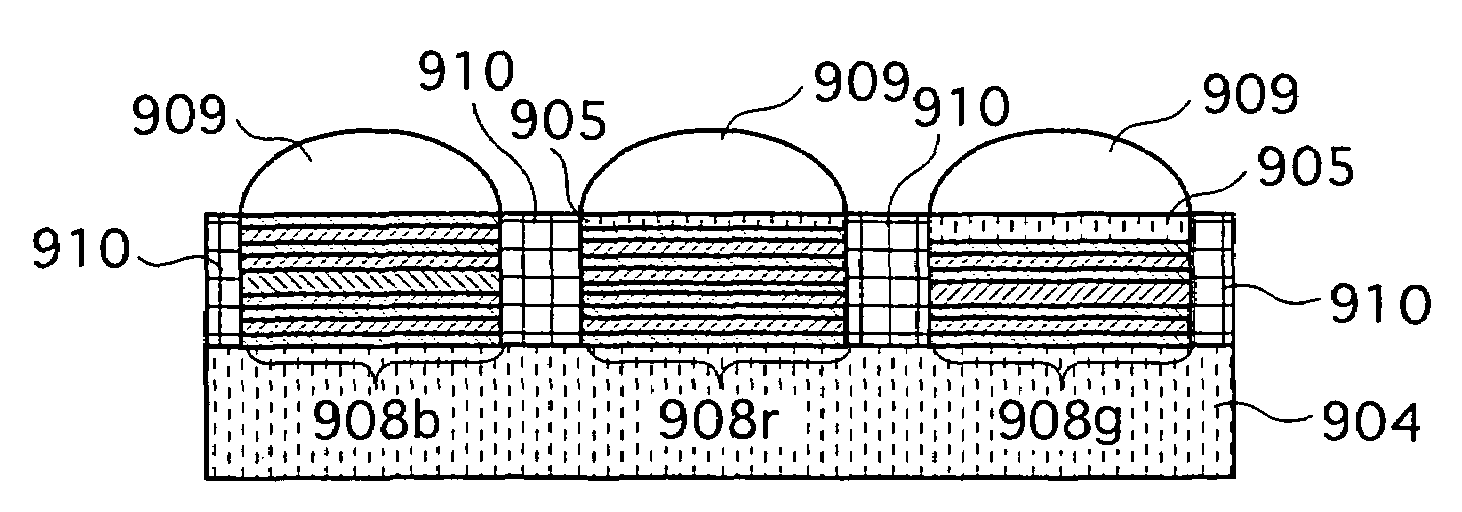
[0047]The following first describes a structure of the solid-state imaging device pertaining to the present embodiment. FIG. 3 is a cross-sectional view showing a portion of a structure of the solid-state imaging device according to embodiment 1 of the present invention. As shown in FIG. 3, a solid-state imaging device 1 includes a semiconductor substrate 101, photoelectric converters 102, a planarizing layer 103, a light shielding layer 104, a planarizing layer 105 and condenser lenses 106.

[0048]The light shielding layer 104 has apertures 104a in which multilayer interference filters 107r, 107g and 107b are disposed.

[0049]The condenser lenses 106 focus incident light onto corresponding photoelectric converters 102. The multilayer interference filters 107r, 107g and 107b selectively transmit specific wavelength components of incident light. The light shielding film 104 prevents light transmitted by the condenser lenses 106 from be...


PUM


Abstract

Photoelectric converters are arranged two-dimensionally in a semiconductor substrate. A planarizing layer, a light shielding film, a further planarizing layer and condenser lenses are formed sequentially on the semiconductor substrate and the photoelectric converters. The light shielding film has apertures at positions corresponding to the photoelectric conversion devices. Multilayer interference filters that transmit either a red, green or blue wavelength component of light are disposed in the apertures.

Description

[0001]This application is based on application No. 2005-009619 filed in Japan, the content of which is hereby incorporated by reference.BACKGROUND OF INVENTION[0002]1. Field of the Invention[0003]The present invention relates to a solid-state imaging device and manufacturing method for the same, and in particular to a technique for preventing color-mixing that occurs as a result of light which has passed through a color filter being incident on the wrong light receiving device.[0004]2. Related Art[0005]Solid-state imaging devices, which are essentially the heart of digital cameras that have become widely used in recent years, take color images by using color filters to separate incident light into its constituent colors. FIG. 1 is a cross-sectional view showing a structure of a solid-state imaging device according to conventional technology.[0006]As shown in FIG. 1, a solid-state imaging device 11 includes a semiconductor substrate 1101 which has photoelectric converters 1102 formed...

Claims


Application Information

Patent Timeline
Patent Type & Authority Patents(United States)
IPC IPC(8): H01L31/0216G02B5/20G02B5/28H01L27/14H04N5/335H04N5/369
CPCG02B5/201G02B5/285H01L27/14621H01L31/02165H01L27/14625H01L27/14685H01L31/02162H01L31/02164H01L27/14623G01J3/513G06V40/12
Inventor KASANO, MASAHIROINABA, YUICHIYAMAGUCHI, TAKUMI
Owner PANASONIC CORP
Why Eureka
Try Eureka