Three inch silicon carbide wafer with low warp, bow, and TTV
a silicon carbide and wafer technology, applied in the field of low defect silicon carbide wafers, can solve the problems of difficult work of silicon carbide, warp, bow and total thickness variation (ttv) introduction in the sliced wafer, and undesirable bow and ttv of the wafer, and achieve the effect of high quality
Active Publication Date: 2008-09-09
CREE INC
View PDF87 Cites 66 Cited by
- Summary
- Abstract
- Description
- Claims
- Application Information
AI Technical Summary
Benefits of technology
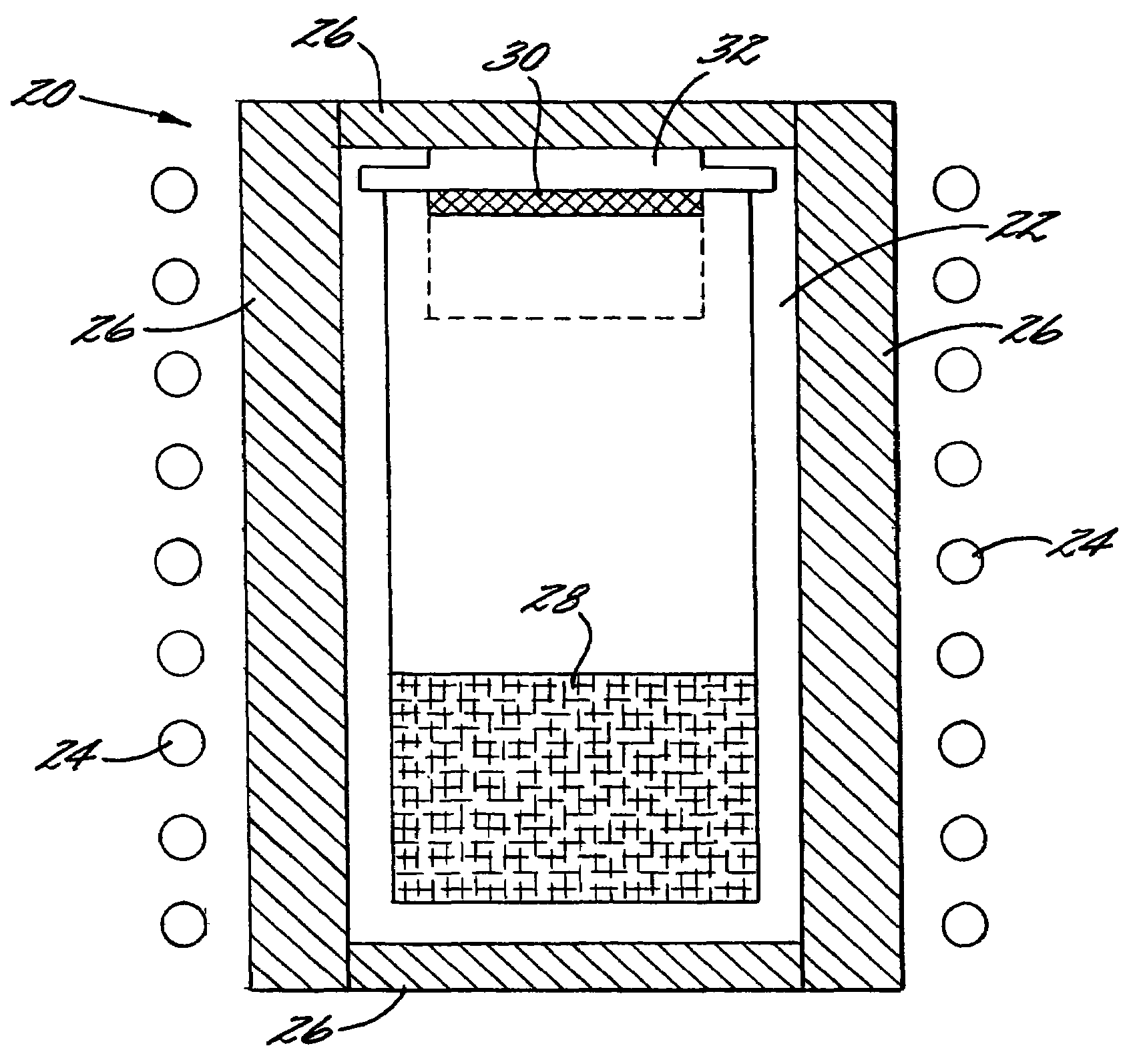
The present invention is a high quality single crystal wafer of SiC with a diameter of at least 3 inches, a warp of less than 0.5 μm, a bow of less than 0.5 μm, and a TTV of less than 1.0 μm. Additionally, the invention is a method of epitaxial growth of SiC or III-V materials on these high quality single crystal wafers of SiC. Furthermore, the invention is a plurality of power, microwave, or LED devices built on a single crystal substrate of SiC with a diameter of at least 3 inches, a warp of less than 0.5 μm, a bow of less than 0.5 μm, and a TTV of less than 1.0 μm.
Problems solved by technology
Silicon carbide is a difficult material to work with because it can crystallize in over 150 polytypes, some of which are separated from one another by very small thermodynamic differences.
One drawback to traditional lapping and slicing techniques is the introduction of warp, bow, and total thickness variations (TTV) in the sliced wafers.
Wafers with high warp, bow and TTV may be undesirable for several reasons.
For example, during epitaxial growth processes, high warp, bow and TTV levels result in uneven contact between the wafer and susceptor.
Such uneven contact may result in thermal variations across the seed during the epitaxial growth process.
Also high warp values may increase the risk of wafer cracking during the device fadrication steps due to the stresses induced as the wafer is sucked down to the vacuum chucks.
Method used
View moreImage
Smart ImageViewing Examples

Examples
examples
[0050]A series of three-inch diameter and approximately one millimeter thick SiC wafers were formed according to the present invention. The warp, bow and TTV of each of these wafers is shown in Table 1.
[0051]
TABLE 1Warp, bow, and TTV of SiC WafersWarpBowTTVWafer(μm)(μm)(μm)10.222−0.1160.62320.147−0.0180.67330.08460.02670.739
Login to View More PUM
| Property | Measurement | Unit |
|---|---|---|
| diameter | aaaaa | aaaaa |
| diameter | aaaaa | aaaaa |
| diameter | aaaaa | aaaaa |
Abstract
A high quality single crystal wafer of SiC is disclosed. The wafer has a diameter of at least about 3 inches, a warp of less than about 5 μm, a bow less than about 5 μm, and a total thickness variation of less than about 2.0 μm.
Description
BACKGROUND OF THE INVENTION[0001]The present invention relates to low defect silicon carbide wafers and their use as precursors for semiconductor purposes, to seeded sublimation growth of large, high-quality silicon carbide single crystals, and to high quality epitaxial growth upon such low defect wafers.[0002]The invention is also related to the following copending and commonly assigned U.S. applications: Ser. No. 10 / 628,189 filed Jul. 28, 2003 for Growth of Ultra-High Purity Silicon Carbide Crystals in an Ambient Containing Hydrogen; Ser. No. 10 / 628,188 filed Jul. 28, 2003 for Reducing Nitrogen Content in Silicon Carbide Crystals by Sublimation Growth in a Hydrogen-Containing Ambient; Ser. No. 10 / 707,898 filed Jan. 22, 2004 for Silicon Carbide on Diamond Substrates and Related Devices and Methods; Ser. No. 60 / 522,326 filed Sep. 15, 2004 for Seed Preparation for the Growth of High Quality Large Size Silicon Carbide Crystals; Ser. No. 10 / 915,095 filed Aug. 10, 2004 for Seed and Seed...
Claims
Login to View More Application Information
Patent Timeline
 Patent Type & Authority Patents(United States)
IPC IPC(8): C01B33/20C30B23/00
CPCC30B23/00C30B29/36C30B33/00H01L21/02378H01L21/0243H01L29/66068H01L21/0254H01L21/02024Y10T428/21H01L29/1608Y10T117/102Y10T117/1004Y10T117/10
Inventor POWELL, ADRIANBRIXIUS, WILLIAM H.LEONARD, ROBERT TYLERMCCLURE, DAVIS ANDREWLAUGHNER, MICHAEL
Owner CREE INC
Features
- Generate Ideas
- Intellectual Property
- Life Sciences
- Materials
- Tech Scout
- Unparalleled Data Quality
- Higher Quality Content
- 60% Fewer Hallucinations
Learn More Browse by: Latest US Patents, China's latest patents, Technical Efficacy Thesaurus, Application Domain, Technology Topic, Popular Technical Reports.
© 2025 PatSnap. All rights reserved.Legal|Privacy policy|Modern Slavery Act Transparency Statement|Sitemap|About US| Contact US: help@patsnap.com