Measuring chip-to-chip capacitance differentials by demodulating signals over a capacitance bridge

a capacitance differential and chip-to-chip technology, applied in the field of electronic circuits, can solve the problems of destroying received signals, increasing the difficulty of capacitance measurement, and existing capacitance-measurement techniques often suffering from limited sensitivity

Active Publication Date: 2008-09-16
ORACLE INT CORP
View PDF2 Cites 12 Cited by
  • Summary
  • Abstract
  • Description
  • Claims
  • Application Information

AI Technical Summary

Problems solved by technology

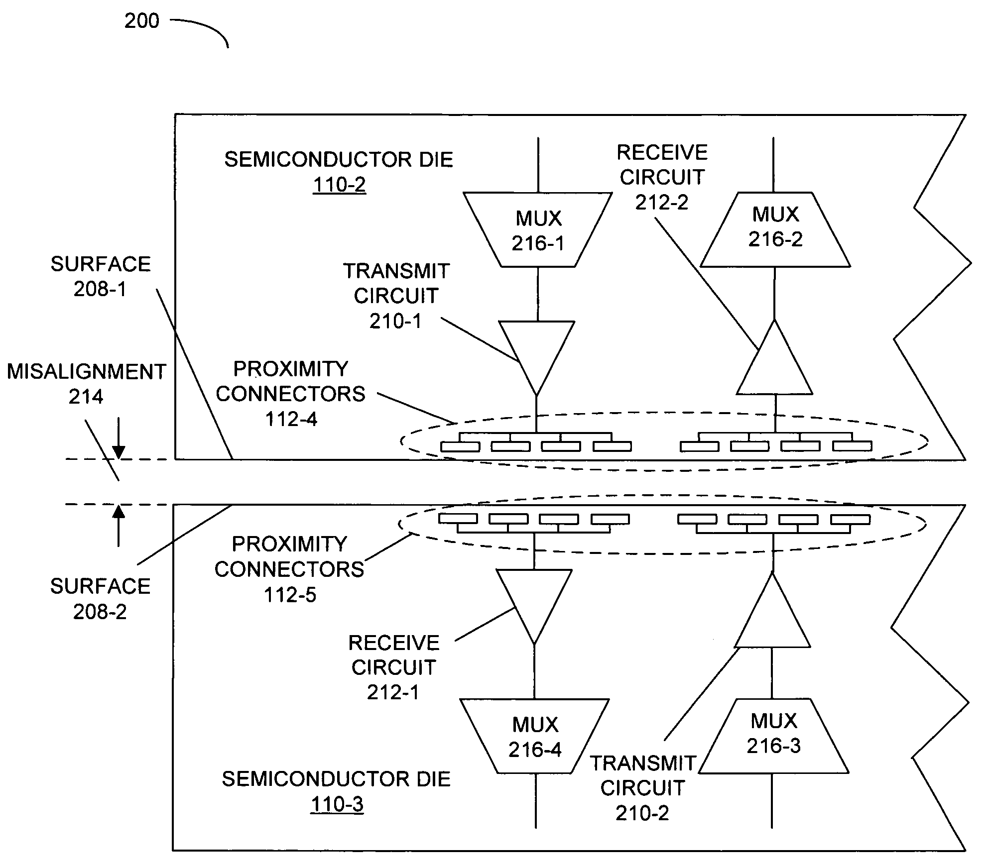
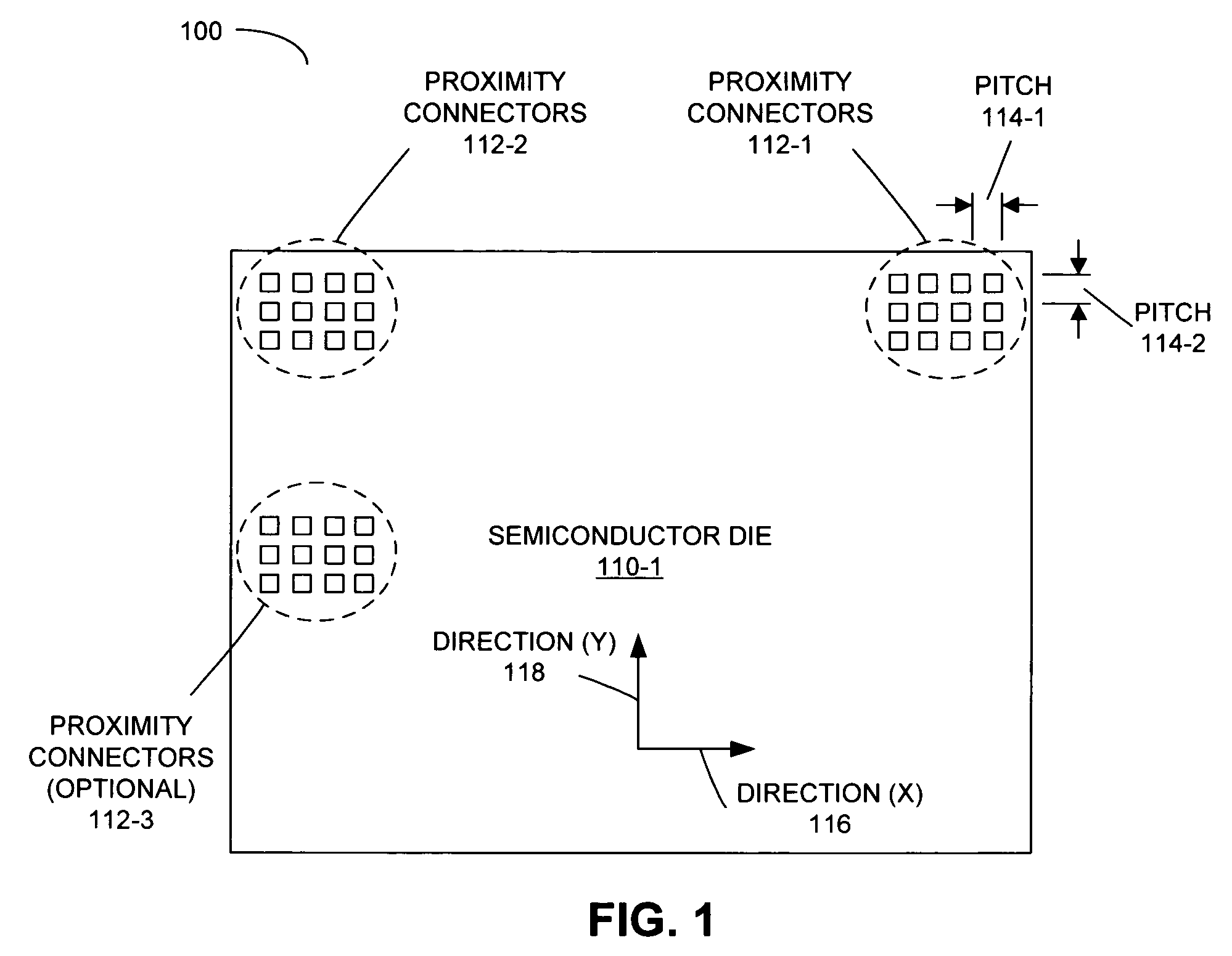
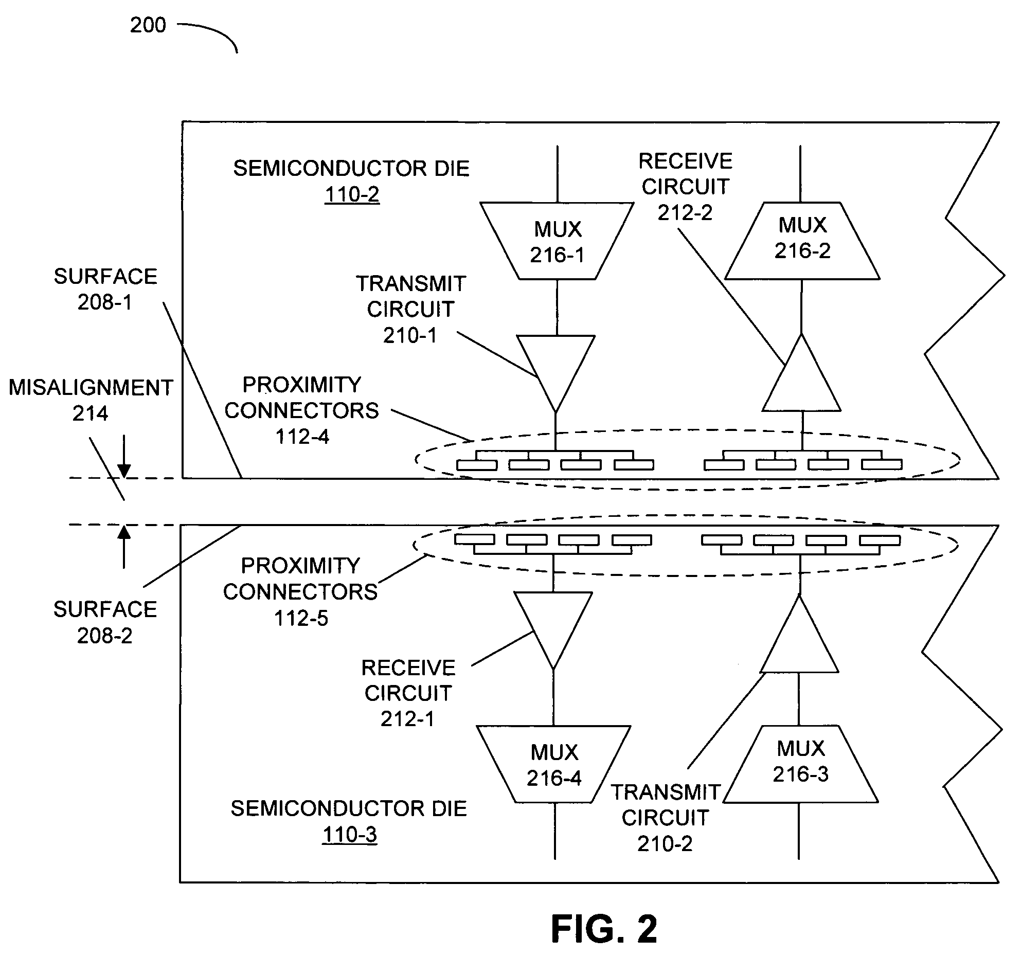
Misalignment between the transmitter pads and the receiver pads may cause each receiving pad to span two transmitting pads, thereby destroying a received signal.
Unfortunately, existing capacitance-measurement techniques often suffer from limited sensitivity.
For example, many techniques involve precise measurements of very small currents, which is becoming increasingly difficult because of the large amounts of transistor leakage current that arise as circuit dimensions continue to decrease.
These leakage currents may cause problems when measuring the capacitances of wires in integrated circuits, which may be extremely small due to submicron dimensions of modern integrated circuit processes.

Method used


Image

  • Measuring chip-to-chip capacitance differentials by demodulating signals over a capacitance bridge
  • Measuring chip-to-chip capacitance differentials by demodulating signals over a capacitance bridge
  • Measuring chip-to-chip capacitance differentials by demodulating signals over a capacitance bridge

Examples


embodiment 450

[0061]Signals that are received on the terminal 414-3 are coupled to a follower or buffer 420. In an exemplary embodiment, the buffer 420 has unity gain. However, in other embodiments (such as embodiment 450) a differential amplifier or a variable-gain amplifier (for example, with a gain approximately between 3 and 10) may be used. The received signals are then coupled to mixer or modulator 422 in which they are demodulated using modulation signal VM(t) 424. In some embodiments, the signal VM(t) 424 is generated by optional signal generator 432 or is provided by a signal generator that is external to the semiconductor die 410-2. The signal VM(t) 424 is periodic and has a fundamental frequency that is the same as the fundamental frequency of the time-varying signals VT(t) 418-1 and -VT(t) 418-2. In exemplary embodiments, the fundamental frequency is between 1 kHz and 3 MHz, and the signal VM(t) 424 is a sine-wave signal, a square-wave signal, or a pseudo-random signal. Demodulation u...

embodiment 400

[0064]While the embodiment 400 illustrates a given configuration, in other embodiments at least a portion of the circuitry may be implemented on a separate Application Specific Integrated Circuit (ASIC), Field Programmable Gate Array (FPGA), or on another circuit board. Furthermore, in some embodiments, at least a portion of the detection circuit (such as the modulator 422 and / or the filter 426) may be implemented using Digital Signal Processing (DSP). Note that if the buffer 420 or amplification is implemented external to the semiconductor die 410-2 (i.e., off-chip), integration over multiple periods corresponding to the fundamental frequency of the time-varying signals VT(t) 418-1 and -VT(t) 418-2 may be used to improve the signal-to-noise ratio.

[0065]In addition, while embodiment 400, and embodiments 440, 450, and 470, is illustrated as having a number of components in a given configuration, other embodiments may include fewer components or additional components, two or more comp...

embodiment 470

[0067]Embodiment 470 illustrates another variation of this measurement technique. The capacitor 416-2 has been replaced by a varactor 480, which has a voltage-controlled variable capacitance. By sequentially varying the capacitance of the varactor 480, the magnitude of the capacitance of the capacitor 416-1 may be determined. Note that in an alternate embodiment an off-chip capacitor may be used as a reference capacitor. This off-chip capacitor may be used in conjunction with or independently of the varactor 480.

[0068]We now discuss the theory underlying the capacitance measurement technique. For a phase of 180° between the time-varying signals VT(t) 418-1 and -VT(t) 418-2, the received signal VR(t) is

[0069]C1-C2C1+C2+Cp⁢VT⁡(t)=Cd⁢VT⁡(t),

where C1 is the capacitance of the capacitor 416-1, C2 is the capacitance of the capacitor 416-2, Cp represents all of the parasitic capacitances in the detection circuit on the semiconductor die 410-2, and Cd is the difference in the coupling capac...


PUM


Abstract

In a method for determining capacitance, a first time-varying signal is driven on a first terminal of a first capacitor and a second time-varying signal is driven on a first terminal of a second capacitor, where the first time-varying signal and the second time-varying signal have a pre-determined phase relationship with each other.These signals are received on second terminals of the first capacitor and the second capacitor and demodulated using a periodic signal to produce demodulated signals. This periodic signal has the same fundamental frequency as the first time-varying signal and the second time-varying signal. A DC component in the demodulated signals is then determined by filtering the demodulated signals, and the sign of the DC component is used to determine a relative capacitance of the first capacitor and the second capacitor.

Description

GOVERNMENT LICENSE RIGHTS[0001]This invention was made with United States Government support under Contract No. NBCH3039002 awarded by the Defense Advanced Research Projects Administration. The United States Government has certain rights in the invention.BACKGROUND[0002]1. Field of the Invention[0003]The present invention relates to electronic circuits. More specifically, the present invention relates to the design of a capacitance-measurement circuit.[0004]2. Related Art[0005]Accurate capacitance models are typically used during the process of designing high-performance integrated circuits. Critical design parameters, such as the delay through logic circuits, the bandwidth of analog circuits, and the power required for cross-chip communication largely depend on wire and device capacitance. Capacitance models often include a combination of physical equations, 2-dimensional or 3-dimensional field simulations, and / or measured capacitances. Typically, physical equations and measured ca...

Claims


Application Information

Patent Timeline
Patent Type & Authority Patents(United States)
IPC IPC(8): G01R27/26
CPCG01R27/26
Inventor CHOW, ALEXHOPKINS, ROBERT D.SCHAUER, JUSTIN M.
Owner ORACLE INT CORP
Why Eureka
Try Eureka