

Method of forming solder resist pattern
- Summary
- Abstract
- Description
- Claims
- Application Information
AI Technical Summary
Benefits of technology
Problems solved by technology
Method used
Image

Examples
Embodiment Construction
[0057]Hereinafter, the present invention will be explained in more detail with reference to the accompanying drawings.
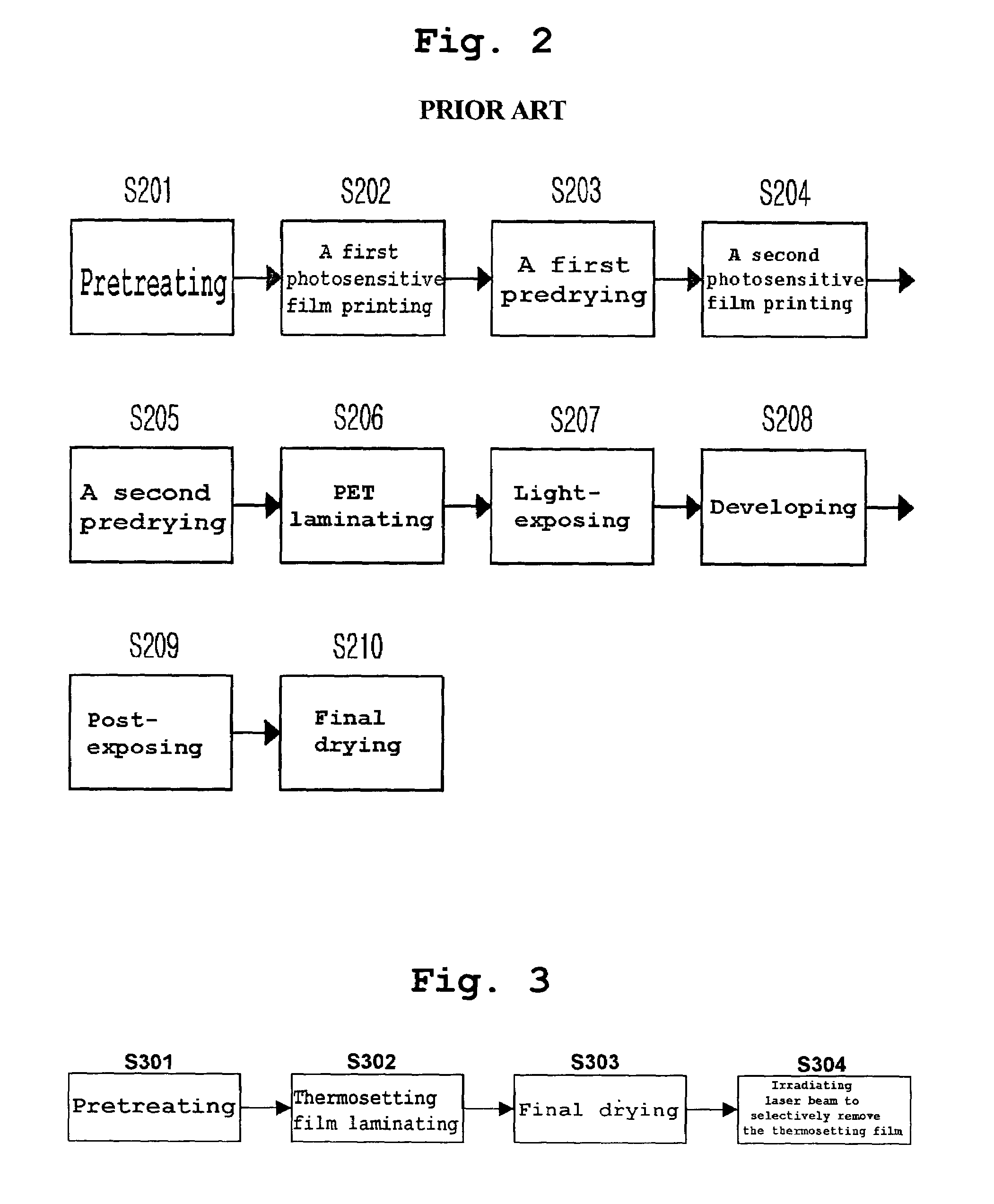
[0058]A flowchart showing a method for forming a solder resist pattern of the present invention is shown in FIG. 3.
[0059]In step S301, a scrubbing process is carried out to improve the adhesion between an insulating thermosetting solder resist film and a substrate.
[0060]When fingerprints, oil, dust, etc., are stuck on the substrate, a solder resist ink is not closely adhered to the substrate, causing a problem of low adhesion. In addition, the incomplete adhesion causes non-uniform plating thickness during plating process, which leads to cutting of wirings or short-circuiting between adjacent wirings. Accordingly, it is necessary to clean the surface of the substrate in order to prevent the defects. The cleaning operation is called a ‘scrubbing’. The reason for the scrubbing is to roughen the surface of the substrate and to facilitate the lamination on the substrate....
PUM
 Abstract
Description
Claims
Application Information