Packaging method of a plurality of chips stacked on each other and package structure thereof

a technology of plurality of chips and stacking, which is applied in the direction of semiconductor devices, semiconductor/solid-state device details, electrical apparatus, etc., can solve the problems of reducing the heat dissipation efficiency and electrical quality of the package, the disadvantage of metal masks being difficult to mass produce, and the disadvantage of high weight and expense, so as to simplify the anti-electromagnetic wave package process and save costs. , the effect of high heat dissipation

Active Publication Date: 2008-10-14
ADVANCED SEMICON ENG INC
View PDF3 Cites 24 Cited by
  • Summary
  • Abstract
  • Description
  • Claims
  • Application Information

AI Technical Summary

Benefits of technology

[0007]The present invention solves the technical problems by using a substrate with a dielectric layer and a metal layer with the chips stacked between the dielectric layer and the metal layer, or between two surfaces of the metal layer. The present invention not only achieves a high heat-dissipating effect and a metal shield effect for the chip, but also simplifies the anti-electromagnetic wave package process of the prior art and saves costs.

Problems solved by technology

Since consumers' requirements of electronic products increase day by day, improving technology for semiconductor manufacture and design of high frequency chips with better functions obviously becomes an important issue in today's research.
For semiconductor packaging of the high frequency chips, serious electromagnetic wave problems occur frequently due to strong electromagnetic waves generated by the high frequency chips in operation, and the electromagnetic waves are transmitted outside through the package body to cause an electromagnetic interference (EMI) problem in nearby electronic devices, and possibly reduce electrical quality and heat-dissipating efficiency of the package.
It is a serious problem of the high frequency semiconductor package.
However, the metal mask has disadvantages of high weight and expense, and causes difficulty in mass production.
The conventional method obviously does not fit in with a package of low weight, low cost, and mass production.
Therefore, developing a packaging method for preventing chips from being interfered by electromagnetic waves and a package structure thereof with package requirements of heat-dissipation, low cost, and low weight is a major issue in the related research field.

Method used


Image

  • Packaging method of a plurality of chips stacked on each other and package structure thereof
  • Packaging method of a plurality of chips stacked on each other and package structure thereof
  • Packaging method of a plurality of chips stacked on each other and package structure thereof

Examples


Embodiment Construction

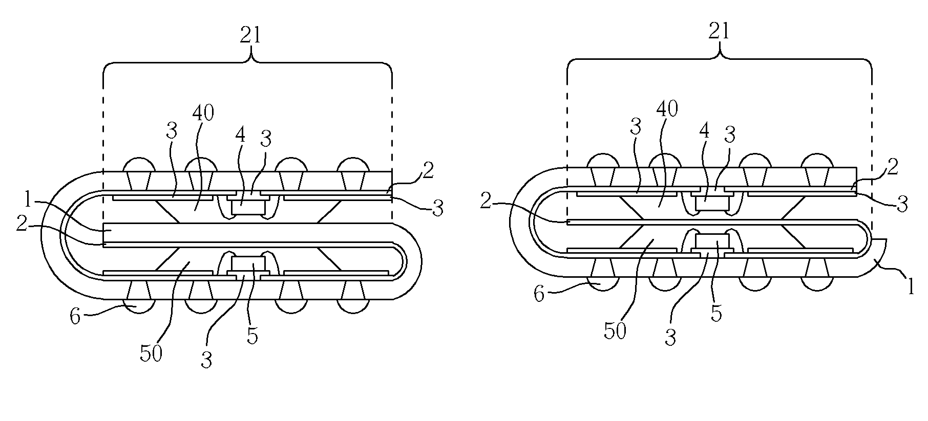
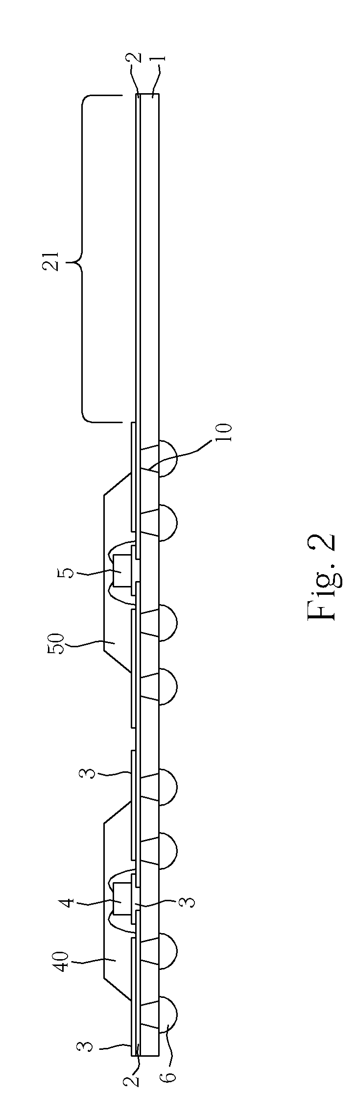
[0019]Please refer to FIG. 1 to FIG. 3. FIG. 1 is a flowchart of the first embodiment of a packaging method of a stack of base band chips and radio frequency (RF) chips according to the present invention. FIG. 2 is a cross-sectional diagram showing a package structure before bending the dielectric layer and the metal layer according to the first embodiment of the present invention. FIG. 3 is a cross-sectional diagram showing a package structure after bending the dielectric layer and the metal layer according to the first embodiment of the present invention.

[0020]As shown in FIG. 1 to FIG. 3, the present invention provides a packaging method of a plurality of chips stacked on each other, and the packaging method includes the following steps. A dielectric layer 1 is provided (S100). Then, a metal layer 2 is formed on the dielectric layer 1, in which the metal layer 2 includes a conducting trace area 20 and a shielding area 21 (S102). Next, a solder mask 3 is formed on the conducting t...


PUM


Abstract

A package structure with a plurality of chips stacked on each other includes a substrate, a first chip and second chip. The substrate has a dielectric layer, a metal layer having a conducting trace area and a shielding area formed on the dielectric layer, and a solder mask formed on the conducting trace area. The first chip and the second chip are electrically connected to the conducting trace area and arranged on the solder mask respectively. The first chip has a package body connected with one surface of the metal layer for arranging the first chip between the solder mask and the shielding area of the metal layer. The second chip has a package body connected with the other surface of the metal layer for arranging the second chip between the solder mask and the shielding area of the metal layer.

Description

BACKGROUND OF THE INVENTION[0001]1. Field of the Invention[0002]The present invention relates to a packaging method of a plurality of chips stacked on each other and a package structure thereof, and more particularly to a packaging method and a package structure that provide a high heat-dissipating effect and a metal shield effect for the chips by using a substrate with a dielectric layer and a metal layer with the chips stacked between the dielectric layer and the metal layer, or between two surfaces of the metal layer.[0003]2. Description of the Prior Art[0004]Since consumers' requirements of electronic products increase day by day, improving technology for semiconductor manufacture and design of high frequency chips with better functions obviously becomes an important issue in today's research. For semiconductor packaging of the high frequency chips, serious electromagnetic wave problems occur frequently due to strong electromagnetic waves generated by the high frequency chips in...

Claims


Application Information

Patent Timeline
Patent Type & Authority Patents(United States)
IPC IPC(8): H01L23/552H01L23/02
CPCH01L23/5387H01L25/0657H01L2224/48091H01L2224/48227H01L2225/0651H01L2225/06579H01L2924/15311H01L2924/3025H01L2924/00014H01L24/48H01L2924/181H01L2924/00012H01L2224/45099H01L2224/45015H01L2924/207
Inventor HU, CHIEH-CHIA
Owner ADVANCED SEMICON ENG INC
Why Eureka
Try Eureka