Efficient method of test and soft repair of SRAM with redundancy

a technology redundancy, applied in the direction of digital storage, instruments, measurement devices, etc., can solve the problems of producer cost risk associated with continued processing of the die, the complexity of the support for two-dimensional redundancy allocation of sram memory array,

Inactive Publication Date: 2008-10-14
GLOBALFOUNDRIES INC
View PDF5 Cites 20 Cited by
  • Summary
  • Abstract
  • Description
  • Claims
  • Application Information

AI Technical Summary

Benefits of technology

[0013]The method and system described herein provides a consistent test flow and repair methodology usable for all levels of assembly test, including a simple data history table. This table is used to track failing locations observed during any level of assembly test of processor or logic semiconductor chips containing SRAM macros with redundant elements for failure relief, by means of Array Built In Self Test (ABIST), or by external test support equipment and data processing. This data history table is then used as the basis for any repair solutions calculated to control the redundant element invocations of the SRAM for failure relief, whether it is from hard blown fuse technologies or a soft latch or register control approach. The only requirement on the SRAM redundancy circuit design is that there is a provision for disabling the repair solutions calculated, if any.

Problems solved by technology

The difficulty encountered at this point is in further data collection of subsequent levels of assembly test, where one must know if the redundant elements were invoked, to properly calculate internal memory array locations of subsequent fails. i.e. were the observed fails shifted from their base positions by the presence of a repair within the memory array.
The problem created here, in terms of multiple levels of test and data collection for purposes of failure relief within the SRAM memory array elements, requires not only maintenance of a fail history of the device under test, but a maintenance of the redundancy configuration of the memory array at the time of that data collection or test point.
The support for two dimensional redundancy allocation is growing more complex for SRAM memory arrays with increased data IO widths (number of data bits into and out of the array) and the increased number of repair actions desired for yield improvement on high speed, high density SRAM products.
In addition it is now an issue to know specifically the configuration of the memory array in terms of the redundant element configurations, for subsequent levels of test and data collection for failure relief within the memory array.
This poses a concern if the test environments are sufficiently different to allow potential AOQL (average outgoing quality level) degradation for the repaired configurations, if subsequent levels of test to determine the original failures are not sufficiently repeated on the repaired configuration.
Also, there is a producer cost risk associated with continued processing of a die that is not guaranteed to function at expected levels until late in the manufacturing process

Method used


Image

  • Efficient method of test and soft repair of SRAM with redundancy
  • Efficient method of test and soft repair of SRAM with redundancy
  • Efficient method of test and soft repair of SRAM with redundancy

Examples


Embodiment Construction

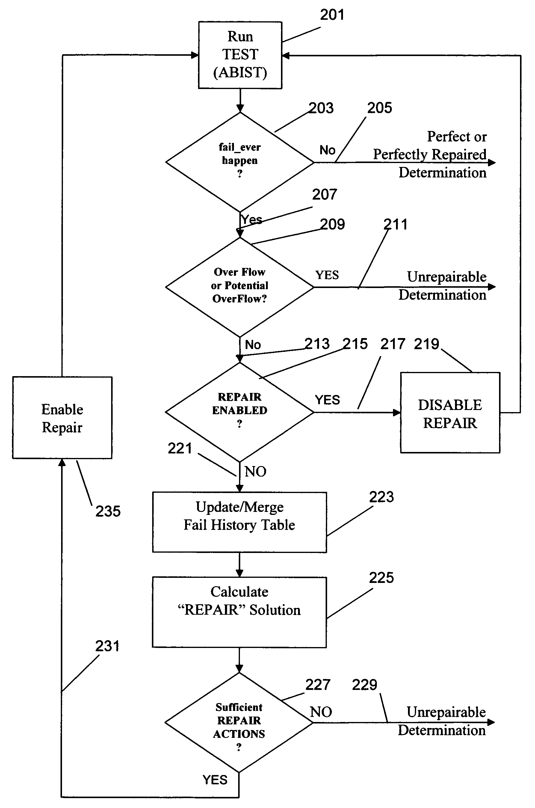
[0018]One preferred embodiment of our invention will be described herein with relation to, but not restricted to, existing ABIST implementations, such as those described in patents which are mentioned below and incorporated herein by reference, including the patents of Huott et al., U.S. Pat. No. 5,633,877 entitled “Programmable Built-In Self-Test Controller for Arrays”, and of Dreibelbis et al., U.S. Pat. No. 5,961,653 entitled “Processor based BIST for an embedded memory” issued Oct. 5, 1999, and the patent of Koch et al, U.S. Pat. No. 5,535,164 for a BIST tester for multiple memories and will further reference this as the ABIST test engine.

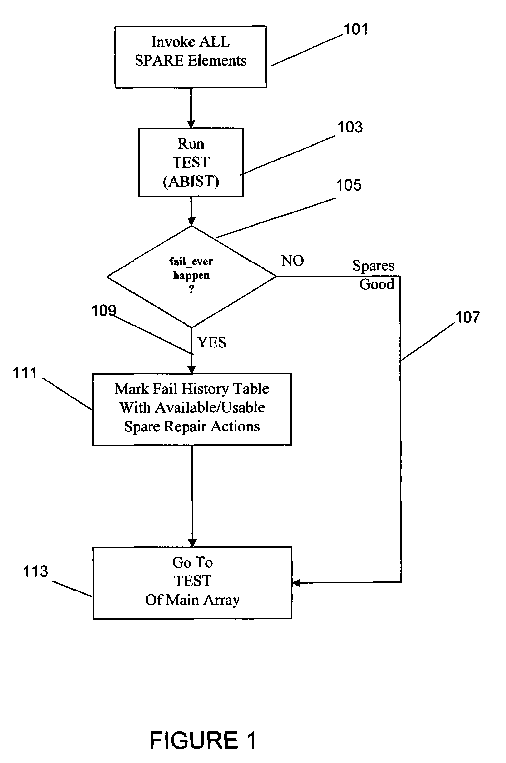
[0019]This preferred embodiment of our proposed methodology, begins with the complete substitution or exposure of the redundant or spare elements provided within the SRAM memory array, as depicted in FIG. 1 for test. This can be accomplished based on the provisions of the architecture of the SRAM memory array, either accessed as part of additio...


PUM


Abstract

Memory array built in self testing utilizing including a simple data history table. The table is used to track failing locations observed during any level of assembly test of processor or logic semiconductor chips where the chips contain SRAM macros with redundant elements for failure relief.

Description

FIELD OF THE INVENTION[0001]The invention described herein relates to memory array built in self testers for random access memory arrays with redundancy circuits for failure relief.BACKGROUND OF THE INVENTION[0002]Traditional testing methodologies of processor or logic semiconductor chips containing SRAM macros with redundant elements for failure relief include Array Built In Self Test (ABIST), and external test support equipment and data processing. These methods involve collection of data from the memory arrays regarding failing locations and some form of on chip fuse and / or latch structures to control the invocations of spare or redundant elements within the memory array elements for failure relief. This is sufficient when the redundant element circuitry performs a straightforward replacement of the defective elements with the memory array structure, enabling the spare elements to become active when a compare of the defective location address to the incoming address to the memory...

Claims


Application Information

Patent Timeline
Patent Type & Authority Patents(United States)
IPC IPC(8): G11C29/00
CPCG11C29/24G11C29/44G11C11/41G11C2029/0401G11C2029/1208G11C2029/4402
Inventor CHANG, TOM Y.HUOTT, WILLIAM V.KNIPS, THOMAS J.PLASS, DONALD W.
Owner GLOBALFOUNDRIES INC
Why Eureka
Try Eureka