
Mask correcting method

a mask and mask technology, applied in the field of mask correction, can solve the problems of large na of the projection optical system of the exposing device, difficult to obtain the desired resolution, and large influence of the dimensional error of the pattern of the photo mask against the transfer pattern,

Inactive Publication Date: 2008-10-21
SONY CORP
View PDF5 Cites 4 Cited by
  • Summary
  • Abstract
  • Description
  • Claims
  • Application Information

AI Technical Summary

Benefits of technology

This approach significantly reduces the residual error in the transferred pattern's dimensional accuracy by matching the line width errors between test and corrected masks, improving the correction accuracy and ensuring the OPE curve remains flat across various pitches.

Problems solved by technology

As a result, NA of a projection optical system of an exposing device is becoming large.
As the required resolution (R) is becoming high, since the k1 factor is becoming low, it becomes difficult to obtain the desired resolution.
Thus, the influence of the dimensional error of a pattern of a photo mask against a transferred pattern is becoming large.
On the other hand, it is very difficult to produce a mask pattern of a photo mask in accordance with its design.
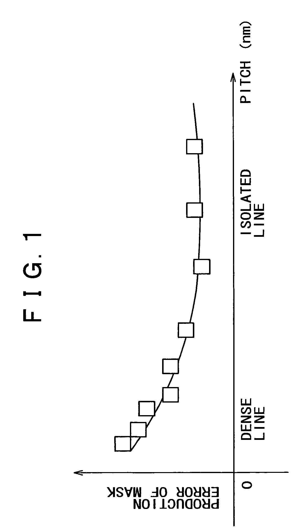
In particular, a problem to be solved is dependency of coarse / dense pattern or an error of line width depending on coarse / dense pattern.
There is a tendency of which the dimensional error of a pattern of dense lines is larger than the dimensional error of a pattern of isolated lines.
196-204, “Advanced pattern correction method for fabricating highly accurate reticles”, although the dimensional error of a pattern of a mask mainly results from a drawing error of a mask pattern and an etching error at an etching step performed after a patterning step and a developing step have been performed, dimension fluctuating coarse / dense characteristic, namely an error of line width depending on coarse / dense pattern is becoming considered.
However, it is difficult to completely control the error of line width depending on coarse / dense pattern.
However, the error of line width depending on coarse / dense pattern has not been mentioned in a roadmap such as ITRS (International Technology Roadmap for Semiconductors).
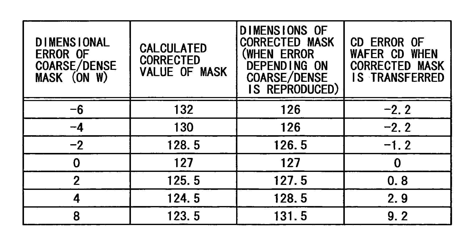
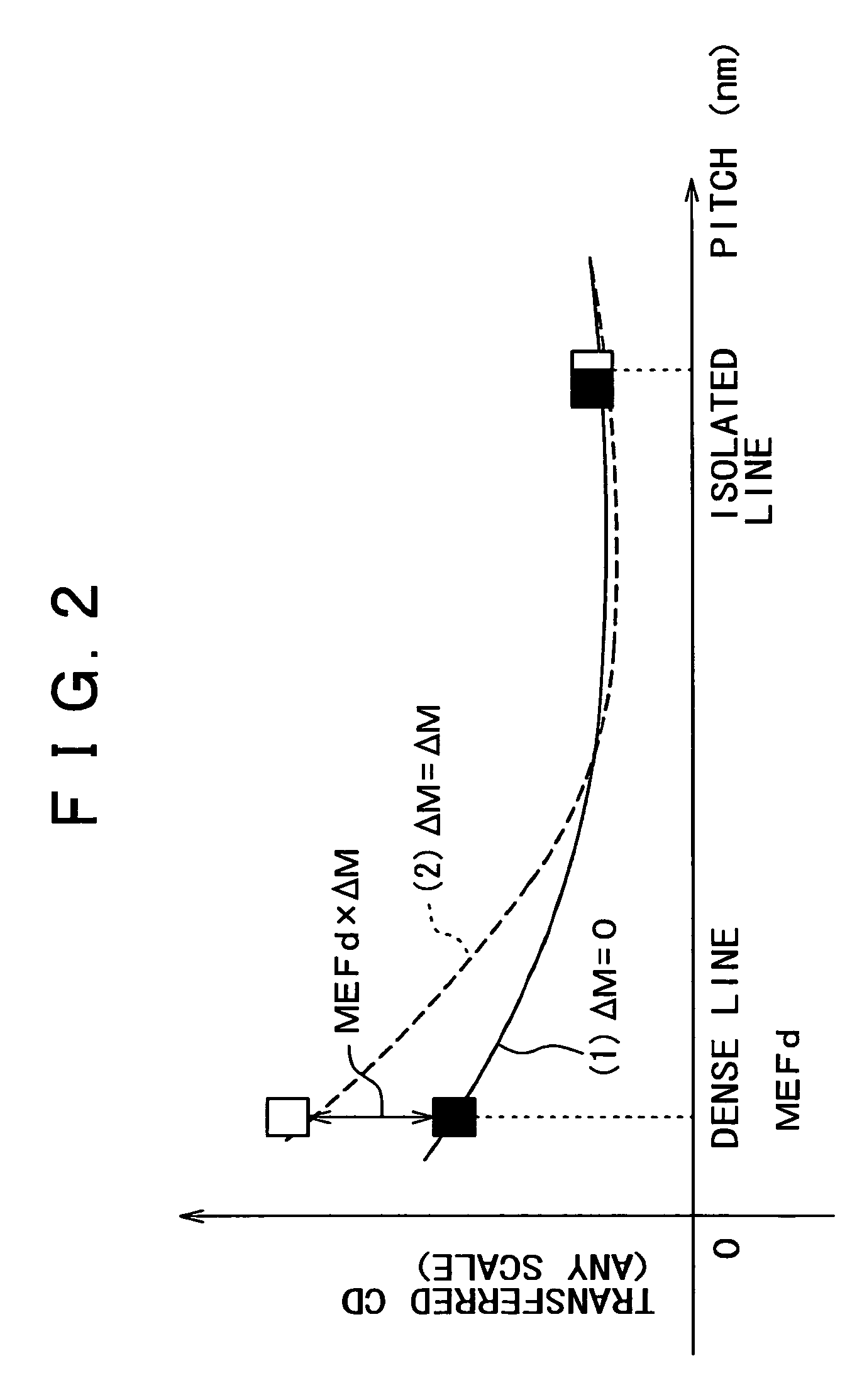
However, as will be described in the following, an error of line width depending on coarse / dense pattern of a mask largely affects a transferred CD error of a transferred pattern.
However, in reality, a mask pattern of a test mask contains an error of line width depending on coarse / dense pattern.
Thus, since a process model that is produced contains a pattern dimension error, an error of line width depending on coarse / dense pattern of a test mask corresponding to an error of line width depending on coarse / dense pattern of a mask is propagated to a process model.
However, in reality, the difference between a test mask and a corrected mask with respect to an error of line width depending on coarse / dense pattern unavoidably takes place in the range of a production error.
As a result, an unignorable error, namely, a mask corrected residual error, takes place in the transferred pattern.
As a result, it becomes difficult to obtain a transferred pattern having a high pattern dimensional control accuracy.
However, in the conventional mask correcting method using the OPC, the difference between masks is not specially considered.
Thus, it becomes difficult to improve the correction accuracy.

Method used


Image

  • Mask correcting method
  • Mask correcting method
  • Mask correcting method

Examples


embodiment

[0102]The embodiment is an example of a mask correcting method according to the present invention. FIG. 7 is a flow chart showing a procedure of the mask correcting method according to the embodiment.

[0103]First of all, at a test mask producing step, step S1, a test mask is produced. The test mask is a mask that functions as a mask for extracting a process model corresponding to the optical proximity effect correction. When the test mask is produced, an allowable range of an error of line width depending on coarse / dense pattern is set in accordance with an analyzed result shown in FIG. 3. Thereafter, a mask producing condition is set so that the error of line width depending on coarse / dense pattern of the test mask is restricted in the allowable range. The test mask is produced in the mask producing condition.

[0104]The mask producing condition for which the test mask is produced the same as a mask producing condition for which the error of line width depending on coarse / dense patter...


PUM

PropertyMeasurementUnit
widthaaaaaaaaaa
widthaaaaaaaaaa
widthaaaaaaaaaa

Abstract

There is provided a method for correcting a photo mask, which allows the difference between a test mask and a corrected mask with respect to an error of line width depending on coarse / dense pattern to be decreased when the photo masks are corrected by optical proximity effect correction.The present method is consisted of: producing a test mask which acts as a mask for extracting process model for applying an optical proximity effect correction method (s1); transferring and measuring the dimensions of the transferred pattern using the test mask (s2 and s3); obtaining a function model (referred to as process model) of which a simulated result of the transferred pattern of a mask pattern of the photo mask using a function model matches the measured result (s4); obtaining a mask pattern of which a transferred pattern matches a designed pattern using said process model and creating mask data in accordance with the obtained mask pattern (s5); producing a corrected mask in accordance with the created mask data (s5); and setting an exposing condition where an OPE characteristic becomes flat with respect of wide and narrow pitches by adjusting at least one of a numerical aperture (NA) and a coherence factor (σ) of an exposing device when the corrected mask is transferred.

Description

[0001]This application claims priority to Japanese Patent Application No. JP2003-037699, filed Feb. 17, 2003 which is incorporated herein by reference.TECHNICAL FIELD [0002]The present invention relates to a method for correcting a photo mask using an optical proximity correction (OPC) method, in particular, to a mask correcting method for removing as much difference between a test mask and a corrected mask with respect to an error of line width depending on coarse / dense pattern.BACKGROUND ART [0003]As a semiconductor device is being miniaturized and highly integrated, a circuit pattern thereof is being miniaturized. As a circuit pattern is becoming miniaturized, in an optical lithography process for patterning a semiconductor device, required resolution is becoming high. As a result, NA of a projection optical system of an exposing device is becoming large. The wavelength of an exposing light source is becoming short.[0004]The resolution (R) in the optical lithography is expressed ...

Claims


Application Information

Patent Timeline
Patent Type & Authority Patents(United States)
IPC IPC(8): G03F1/00G03C5/00G03F1/36G03F1/68G03F9/00G06K9/00H01L21/027
CPCG03F1/36G03F1/144G03F1/44G03F1/68G03F1/84
Inventor OZAWA, KEN
Owner SONY CORP
Learn More