Double feedback rotary traveling wave oscillator driven sampler circuits

a sampler circuit and rotary traveling wave technology, applied in the field of analog to digital converters, can solve the problems of increasing the potential error, slowing down the circuitry, and the precision of existing sample and hold circuits, and achieves the effects of low jitter, minimal effect, and precise timing control of switches

Active Publication Date: 2008-10-21
ANALOG DEVICES INC
View PDF26 Cites 18 Cited by
  • Summary
  • Abstract
  • Description
  • Claims
  • Application Information

AI Technical Summary

Benefits of technology

[0016]One advantage of the present invention is that precise timing control of the switches is possible via the many phases that are available from the rotary traveling wave clock. This precise timing control allows the sampling window to be a precise value.
[0017]Yet another advantage of the present invention is that there is minimal effect on the rotary clock due to the arrangement of the holding capacitor and the second switch. This helps to preserve the favorable characteristics, including low jitter, of the rotary clock for the circuit.
[0018]Yet another advantage of the present invention is that the second switch can be a large semiconductor device when the auxiliary switch is used, because the second switch changes state with practically no voltage across it.
[0019]Yet another advantage is that an A to D circuit can be built with more bits of precision because of the low noise and precise timing characteristics of the rotary traveling wave clock.

Problems solved by technology

Existing sample and hold circuits have a problem with precision due to aperture jitter.
This is an especially difficult problem when the input waveform is a high slew rate signal.
The higher the frequency of the input voltage, the greater the potential error.
In addition to the time uncertainty of the sampling window, inaccurate timing for defining the window means that part of the sampling interval is used up, thereby slowing the circuitry down.
Another problem with the existing art is signal feedthough from the analog input due to parasitic capacitances of the MOSFET device.
A deficiency of this approach is that the high voltage output may be greater than the supply voltage, Vdd, creating problems with the operation of the sampling switch when implemented as a MOSFET device.

Method used


Image

  • Double feedback rotary traveling wave oscillator driven sampler circuits
  • Double feedback rotary traveling wave oscillator driven sampler circuits
  • Double feedback rotary traveling wave oscillator driven sampler circuits

Examples


Embodiment Construction

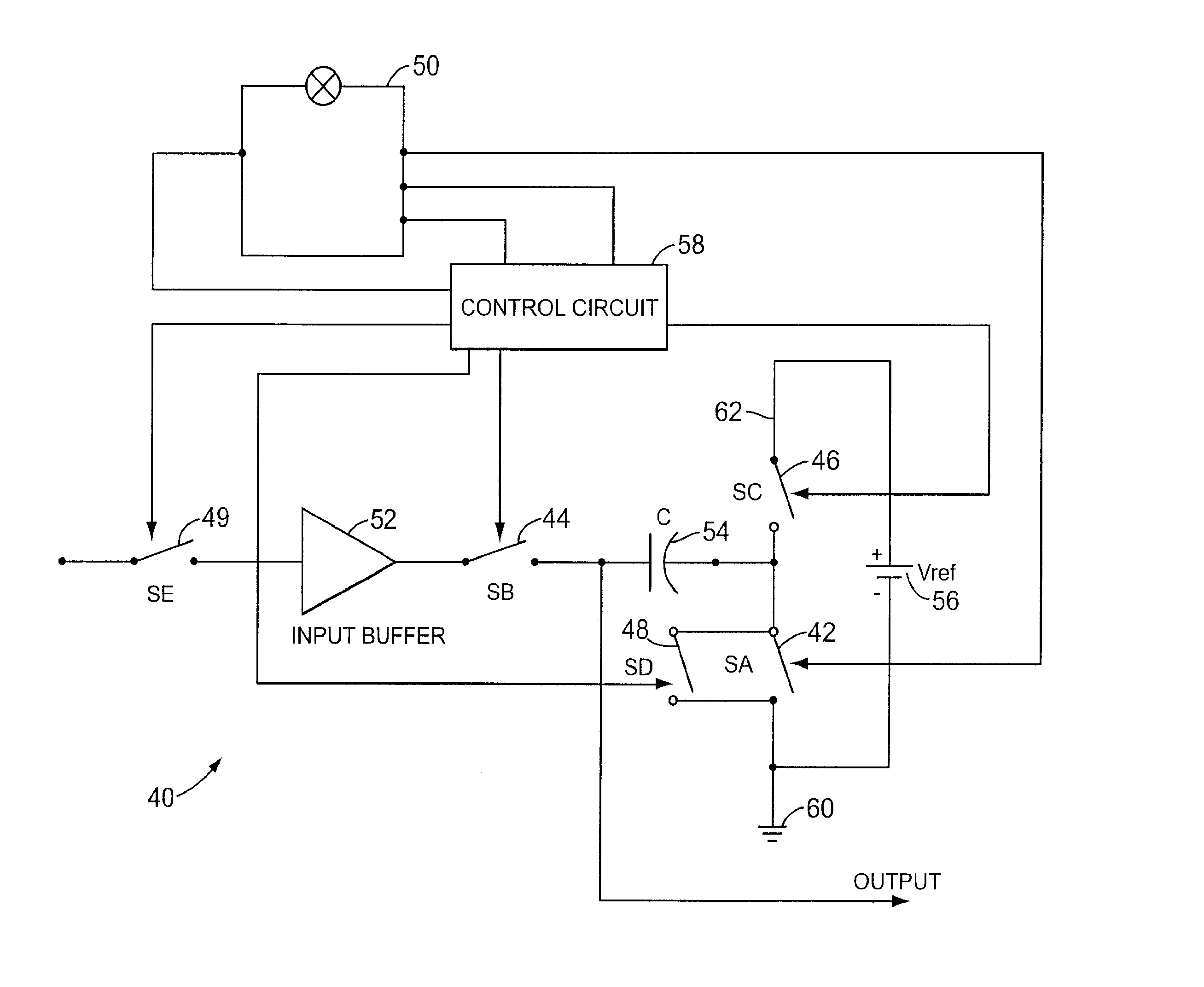
[0034]FIG. 3 shows an embodiment 40 of the present invention. The sampling system 40 includes switches SA 42, SB 44, SC 46, SD 48 and SE 49, a rotary clock oscillator 50 (described in U.S. Pat. No. 6,556,089), an input buffer 52, a sampling capacitor 54, a voltage reference 56, and control circuitry 58.

[0035]Switch SE 49 connects the input analog voltage to the input buffer 52. Switch SB 44 connects the output of the input buffer 52 to a first node of the charging capacitor C 54. Switch SA 42 connects a second node of the charging capacitor 54 to a ground reference node 60. Switch SC 46 connects the second node of the charging capacitor 54 to a voltage reference node 62. Switch SD 48 is connected in parallel with switch SA 42, and is discussed below. The voltage reference Vref 56 can be any voltage, including the ground potential. The rotary clock oscillator 50 and control circuit 58 provide the clock taps and timing controls for the various switches.

Operation

[0036]Referring to FIG....


PUM


Abstract

A sampling circuit and method are disclosed. The sampling circuit includes a buffer, a holding capacitor, a set of switches, and at least two voltage references. The buffer drives buffered analog input signal via a first switch to a first node of holding capacitor. A second switch connects a second node of the holding capacitor to a first reference voltage. A third switch connects the second node of the holding capacitor to a second reference voltage. When the first and second switches are closed, charge accumulates on the holding capacitor. Opening the second switch terminates charging. The third switch biases the charged capacitor to the second reference voltage and the sampled output is taken from the first node of the holding capacitor. A rotary clock and control circuit provide the precise timing for the switches, especially the opening of the second switch, which determines the end of the sampling time.

Description

CROSS-REFERENCE TO RELATED APPLICATIONS[0001]This application incorporates by reference U.S. Pat. No. 6,556,089.[0002]This application claims priority to and incorporates by reference Great Britain Application GB0416803 AO, titled “ROTARY FLASH ADC, filed on Jul. 27, 2004, in Great Britain.FIELD OF THE INVENTION[0003]The present invention relates generally to analog to digital converters and more particularly to the sample and hold circuitry used therein.DESCRIPTION OF THE RELATED ART[0004]In analog to digital conversion (ADC) systems, when a conversion is performed, an analog signal must be sampled at an instant in time and then held while a digital equivalent of the signal is computed. FIG. 1 shows a convention dual-slope A / D conversion system, which includes an integrator 12, with integration capacitor 14 and integration resistor 16, comparator 18, voltage reference, digital pulse generator 22 and binary counter 24. Also included are switches S126 and S228 for controlling the var...

Claims


Application Information

Patent Timeline
Patent Type & Authority Patents(United States)
IPC IPC(8): G11C27/02H03K17/00H03K5/00
CPCG11C27/026
Inventor WOOD, JOHN
Owner ANALOG DEVICES INC
Why Eureka
Try Eureka