Semiconductor device for use as multimedia memory card, has encapsulant with chamfer such that portion of substrate and chamfer are exposed from encapsulant and remaining portion of surface of substrate is covered by encapsulant

a multimedia memory and semiconductor technology, applied in the direction of printed circuit manufacturing, printed circuit aspects, basic electric elements, etc., can solve the problems of limiting the location and size of chips and passive components that can be mounted on the substrate, conventional mmc failing to meet the memory capacity requirement, and conventional saw singulation equipment not suitably applied to singulation process

Inactive Publication Date: 2008-10-28
SILICONWARE PRECISION IND CO LTD
View PDF6 Cites 70 Cited by
  • Summary
  • Abstract
  • Description
  • Claims
  • Application Information

AI Technical Summary

Benefits of technology

[0008]In light of the foregoing drawbacks in the conventional technology, an objective of the present invention is to provide a semiconductor device for accommodating large chips and a fabrication method thereof, whereby surface area of a substrate can be completely used for mounting chips and passive components without being limited by a molding process.
[0010]Still another objective of the present invention is to provide a semiconductor device for accommodating large chips and a fabrication method thereof, allowing the semiconductor device to be cost-effectively fabricated.
[0014]The package of the semiconductor device in the present invention is shaped only by linear cutting without the use of water jetter or laser cutting technique to form a chamfer as in the conventional technology, such that conventional saw singulation equipment is suitably used in a singulation process in the present invention. Since an area of the carrier covered by the encapsulant is larger than surface area of the substrate, and only the portion of the substrate located between the slanted side thereof and the cutaway corner of the encapsulant is not covered by the encapsulant, a part of the carrier being clamped by a mold used in a molding process for forming the encapsulant, except the portion of the substrate to be exposed from the encapsulant, is located outside the substrate rather than occupying the surface area of the substrate for mounting chips and passive components. As such, large chips such as flash memory chips of 1 Gb can be placed on the substrate to provide high memory capacity for the semiconductor device. Further as the area of the carrier covered by the encapsulant is larger than the surface area of the substrate, this forms an interference-free space where mold flow of a resin compound for making the encapsulant is not interfered with the chip and the passive component during the molding process, thereby preventing uneven mold flow and formation of voids in the encapsulant. More particularly, the arrangement of chip and passive component on the substrate does not affect a path of the mold flow, such that the surface area of the substrate can be completely and well utilized.

Problems solved by technology

However, such method of reducing the area for mounting the chips and passive components limits the location and size of the chips and passive components that can be mounted on the substrate.
As a result, under a condition that memory chips are enlarged in size with increase in capacity of memory cards, a flash memory chip having large capacity of e.g. 1 Gb is deemed oversized and cannot be accommodated on the foregoing substrate, making the conventional MMC fail to meet the requirement of memory capacity.
However, conventional saw singulation equipment is not suitably applied to a singulation process of the above MMC with the substrate 21 being completely covered by the encapsulant 20 because the conventional saw singulation equipment can only perform linear cutting but fails to form a chamfer necessary for the MMC.
However, the use of water jetter or laser cutting technique increases fabrication costs and consumes much material in the cutting process, thereby not favorable for a cost-down strategy of the market.

Method used


Image

  • Semiconductor device for use as multimedia memory card, has encapsulant with chamfer such that portion of substrate and chamfer are exposed from encapsulant and remaining portion of surface of substrate is covered by encapsulant
  • Semiconductor device for use as multimedia memory card, has encapsulant with chamfer such that portion of substrate and chamfer are exposed from encapsulant and remaining portion of surface of substrate is covered by encapsulant
  • Semiconductor device for use as multimedia memory card, has encapsulant with chamfer such that portion of substrate and chamfer are exposed from encapsulant and remaining portion of surface of substrate is covered by encapsulant

Examples


first preferred embodiment

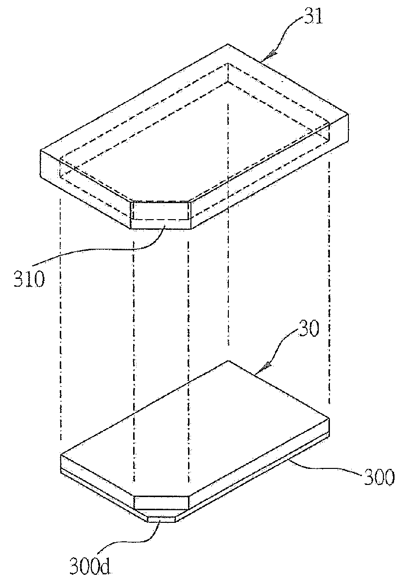
[0031]As shown in FIGS. 3A and 3B, the semiconductor device 3 for accommodating large chips according to a first preferred embodiment of the present invention comprises a package 30 and a lid 31 for covering the package 30. As the combination of package 30 and lid 31 is well known in the art, it is not to be further detailed herein.

[0032]The package 30 comprises a substrate 300; a passive component 301, a controller chip 302 and a memory chip 303, which are mounted on an upper surface 300a of the substrate 300; gold wires 304, 305 for electrically connecting the controller chip 302 and the memory chip 303 to the substrate 300 respectively; and an encapsulant 306 formed on the substrate 300 for encapsulating the passive component 301, the controller chip 302, the memory chip 303, and the gold wires 304, 305.

[0033]A lower surface 300b opposite to the upper surface 300a of the substrate 300 is formed with a plurality of electrical connection terminals 300c exposed from the substrate 30...

second preferred embodiment

[0043]FIG. 5A is a cross-sectional view of a semiconductor device 5 in accordance with a second preferred embodiment of the present invention. The semiconductor device 5 is substantially the same in structure as the semiconductor device 3 of the first embodiment, with the difference in that, sides 506b of an encapsulant 506 of the semiconductor device 5 are not coplanar with sides 500f of a substrate 500 but are slanted inwardly, making the cross-section of the encapsulant 506 have a wedge shape. As shown in FIG. 5B, the encapsulant 506 covers substantially the entire surface area of the substrate 500 except an exposed portion 500e located between a slanted side 500d of the substrate 500 and a cutaway corner 506a of the encapsulant 506, that is, the area for forming the encapsulant 506 does not exceed the substrate 500. During a singulation process for fabricating a package 50 of the semiconductor device 5, saw singulation equipment (not shown) does not cut the encapsulant 506, ther...


PUM


Abstract

A semiconductor device and a fabrication method thereof are provided. An opening having at least one slanted side is formed on a substrate. At least one chip and at least one passive component are mounted on the substrate. An encapsulant having a cutaway corner is formed on the substrate to encapsulate the chip and the passive component, wherein the cutaway corner of the encapsulant is spaced apart from the slanted side of the opening by a predetermined distance. A singulation process is performed to cut the encapsulant to form a package with a chamfer. The package is embedded in a lid to form the semiconductor device, wherein a portion of the substrate located between the slanted side of the opening and the cutaway corner of the encapsulant is exposed from the encapsulant to form an exposed portion. The present invention also provides a carrier for the semiconductor device.

Description

FIELD OF THE INVENTION[0001]The present invention relates to semiconductor devices and fabrication methods thereof, and more particularly, to a semiconductor device incorporated with a plurality of chips to serve as a memory card, and a method for fabricating the semiconductor device.BACKGROUND OF THE INVENTION[0002]Conventional multimedia memory card (MMC) has been disclosed by U.S. Pat. No. 6,040,622. As shown in FIG. 1A (PRIOR ART), the MMC 1 comprises a package 10 embedded in a lid 11 wherein conductive terminals (or gold fingers) 101 formed on a bottom surface 100a of a substrate 100 of the package 10 are exposed to the atmosphere, and the MMC 1 has a chamfer 13 for identifying a direction of application.[0003]As shown in FIG. 1B (PRIOR ART), the package 10 embedded in the lid 11 comprises the substrate 100; a plurality of passive components 102 mounted at predetermined positions of the substrate 100; a flash memory chip 103; a controller chip 104; a plurality of gold wires 105...

Claims


Application Information

Patent Timeline
Patent Type & Authority Patents(United States)
IPC IPC(8): H01L23/06H01L23/04H01L23/12H01L23/28
CPCH01L21/565H01L23/04H01L23/3121H01L24/97H01L25/16H01L25/18H01L25/50H05K3/284H01L2224/48091H01L2224/97H01L2924/01027H01L2924/01079H01L2924/15162H01L2924/19105H05K2201/09127H01L2224/85H01L2924/00014H01L24/48H01L2924/01005H01L2924/01006H01L2924/01033H01L2224/45144H01L2924/00H01L24/45H01L2924/181H01L24/49H01L2224/49171H01L2224/49175H01L2924/00012
Inventor TSAI, YUN-LUNGTSAI, YU-CHIEHCHEN, CHIEN-CHIHHUANG, CHIEN-PING
Owner SILICONWARE PRECISION IND CO LTD
Why Eureka
Try Eureka