Transmission line and wiring forming method

a technology of transmission line and wiring, which is applied in the direction of waveguides, waveguide type devices, high frequency circuit adaptations, etc., can solve the problems of increasing the attenuation value of a signal, the inability and the difficulty of long-distance transmission, so as to increase the wiring width and line interval, increase the characteristic impedance, and reduce the effect of the characteristic impedan

Inactive Publication Date: 2008-11-04
NEC CORP
View PDF4 Cites 8 Cited by
  • Summary
  • Abstract
  • Description
  • Claims
  • Application Information

AI Technical Summary

Benefits of technology

[0014]The present invention is made in view of the above situation and its object is to provide a transmission line and a wiring forming method capable of absorbing reflection caused by mismatching between impedances and restraining the attenuation value of a signal.
[0018]The transmission line's width may be broadened in a wiring area where space for wiring is easily secured.
[0028]In accordance with the wiring forming method, on the printed circuit board, a wiring width may be decreased in a wiring area where space for wiring is difficult to secure and the characteristic impedance of the lines may be adjusted to a predetermined value.
[0029]In accordance with the wiring forming method, a line width may be increased in a wiring area where space for wiring is easily secured on the printed circuit board.
[0037]In the case of a transmission line and a wiring forming method of the present invention, a wiring is designed so as to gradually increase a wiring width and a line interval outside a wiring area where space for wiring is difficult to secure and gradually decrease the characteristic impedance, and also designed so as to gradually decrease a wiring width and a line interval and gradually increase the characteristic impedance of the wiring. Thereby, it is possible to absorb the reflection caused by impedance mismatching and restrain the attenuation value of signals.

Problems solved by technology

To connect a wiring to the high-density connector terminals, a wiring width should be decreased and there arises a problem that the wiring width cannot be increased. FIG. 2 shows attenuation values of a signal according to a difference between wiring width.
Therefore, as shown in FIG. 2, as a wiring width decreases, the attenuation value of a signal increases and thus it becomes difficult to perform long-distance transmission.
In the case of high-speed transmission exceeding GHz, a problem that a signal is attenuated due to dielectric loss and conductor loss of a wiring pattern is generally known.

Method used


Image

  • Transmission line and wiring forming method
  • Transmission line and wiring forming method
  • Transmission line and wiring forming method

Examples


second embodiment

(Second embodiment)

[0088]Then, a second embodiment is described.

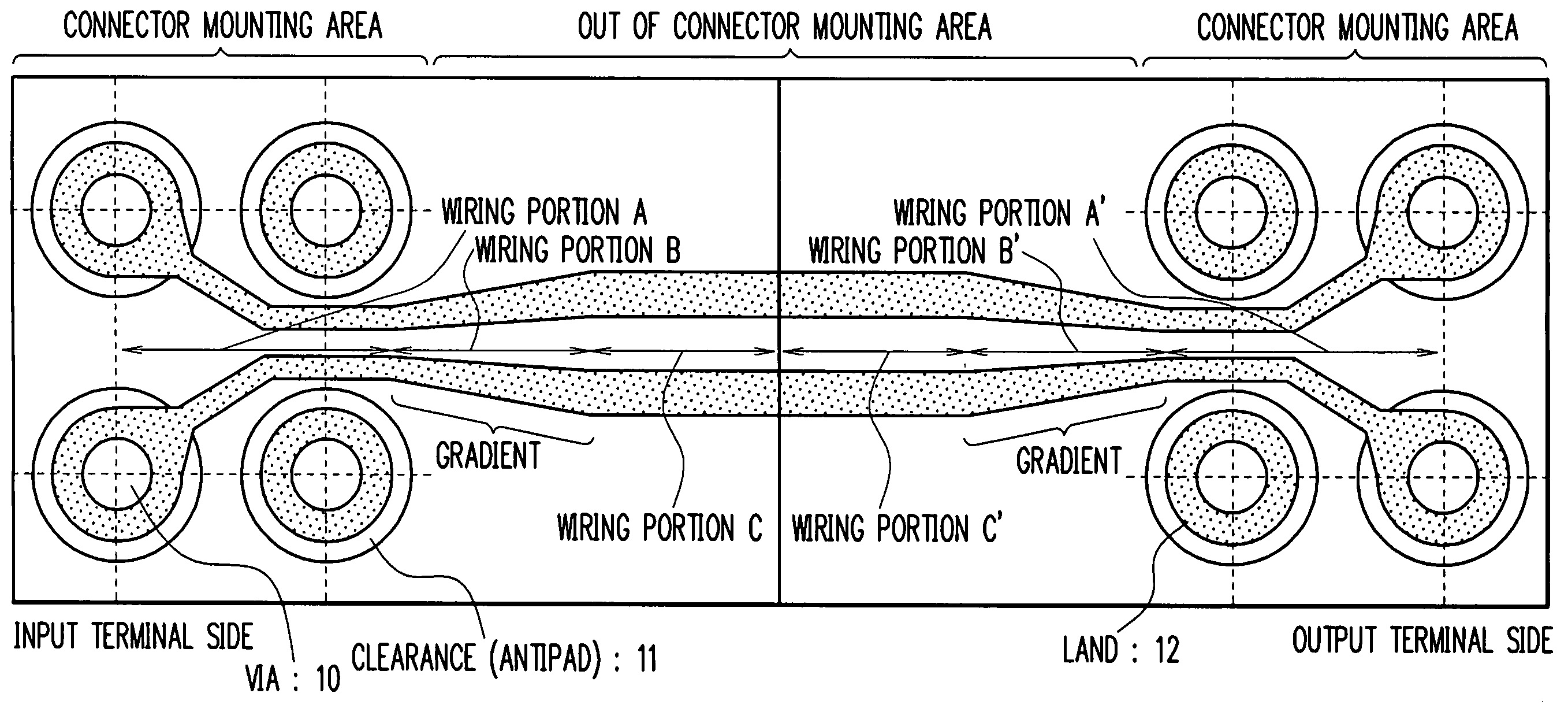
[0089]The transmission line of the first embodiment is designed so as to gradually increase a wiring width like the wiring portion (B) shown in FIG. 3 in order to hold a characteristic impedance gradient. However, for the transmission line of the second embodiment, a characteristic impedance gradient to the wiring width of the wiring portion (B) is optimized by using the expressions (2) and (3) in the case of the microstrip line shown in FIG. 7 and by using the expressions (4) and (5) in the case of the strip line shown in FIG. 8.

[0090]Thus, the transmission line of the second embodiment optimizes the characteristic impedance of a wiring in accordance with the line width w, the line interval s, the thickness t of a wiring layer, the thickness h of an insulating layer, and relative dielectric constant ∈r of an insulating layer in the case of the microstrip ling shown in FIG. 7, and the characteristic impedance of a wirin...


PUM


Abstract

To provide a transmission line capable of absorbing the reflection caused by mismatching between impedances and restraining the attenuation value of a signal. The following wiring patterns are formed out of a connector mounting area in which a connector is mounted: a wiring pattern designed so as to gradually increase the wiring width and the interval between wirings of a wiring portion (B) and gradually decrease the characteristic impedance of the wiring portion (B) and a wiring pattern designed so as to gradually decrease the wiring width and the interval between wirings of the wiring portion (B′) and gradually amplify the characteristic impedance of the wiring portion (B′).

Description

BACKGROUND OF THE INVENTION[0001]The present invention relates to a transmission line applicable to a high-speed backplane transmission and a wiring forming method for forming the wiring of the transmission line.DESCRIPTION OF RELATED ART[0002]Data quantity flowing through an IP network increases year by year because of rapid spread of the Internet. To process the enormous data quantity, high-speed signal processing is performed in an IP switch router. A schematic configuration of the IP switch router is described by referring to FIG. 1.[0003]As shown in FIG. 1, a circuit card (1) and switch card (2) are housed in the housing of an IP switch and they are electrically connected through a backplane (3).[0004]An external circuit signal enters the circuit card (1) in the form of light or electricity, routes are changed by the switch card (2), and a circuit signal is transferred to the outside from another circuit card.[0005]Because in the IP switch router a signal is transferred between...

Claims


Application Information

Patent Timeline
Patent Type & Authority Patents(United States)
IPC IPC(8): H03H7/38
CPCH05K1/0245H05K1/025H05K1/0251H05K1/116H05K2201/09236H05K2201/09727H05K2201/10189
Inventor KASHIWAKURA, KAZUHIRO
Owner NEC CORP
Why Eureka
Try Eureka