Electrostatic induction conversion device
a conversion device and electrostatic induction technology, applied in generators/motors, variable capacitors, instruments, etc., can solve the problems of low processing efficiency, increased thickness of electrets, and inability to work into fine shapes, etc., and achieve high conversion efficiency
- Summary
- Abstract
- Description
- Claims
- Application Information
AI Technical Summary
Benefits of technology
Problems solved by technology
Method used
Image
Examples
embodiment 1
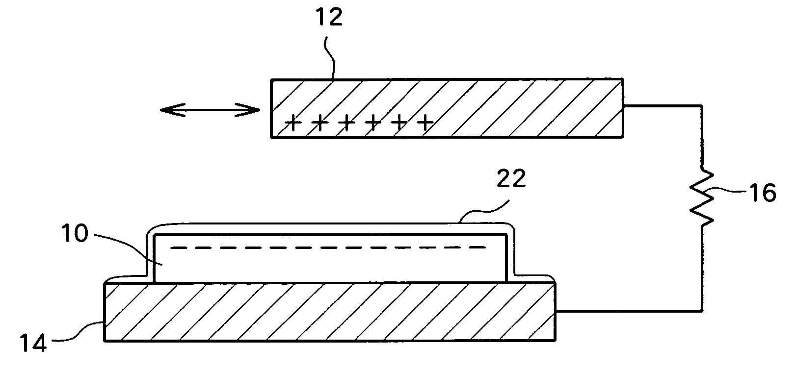
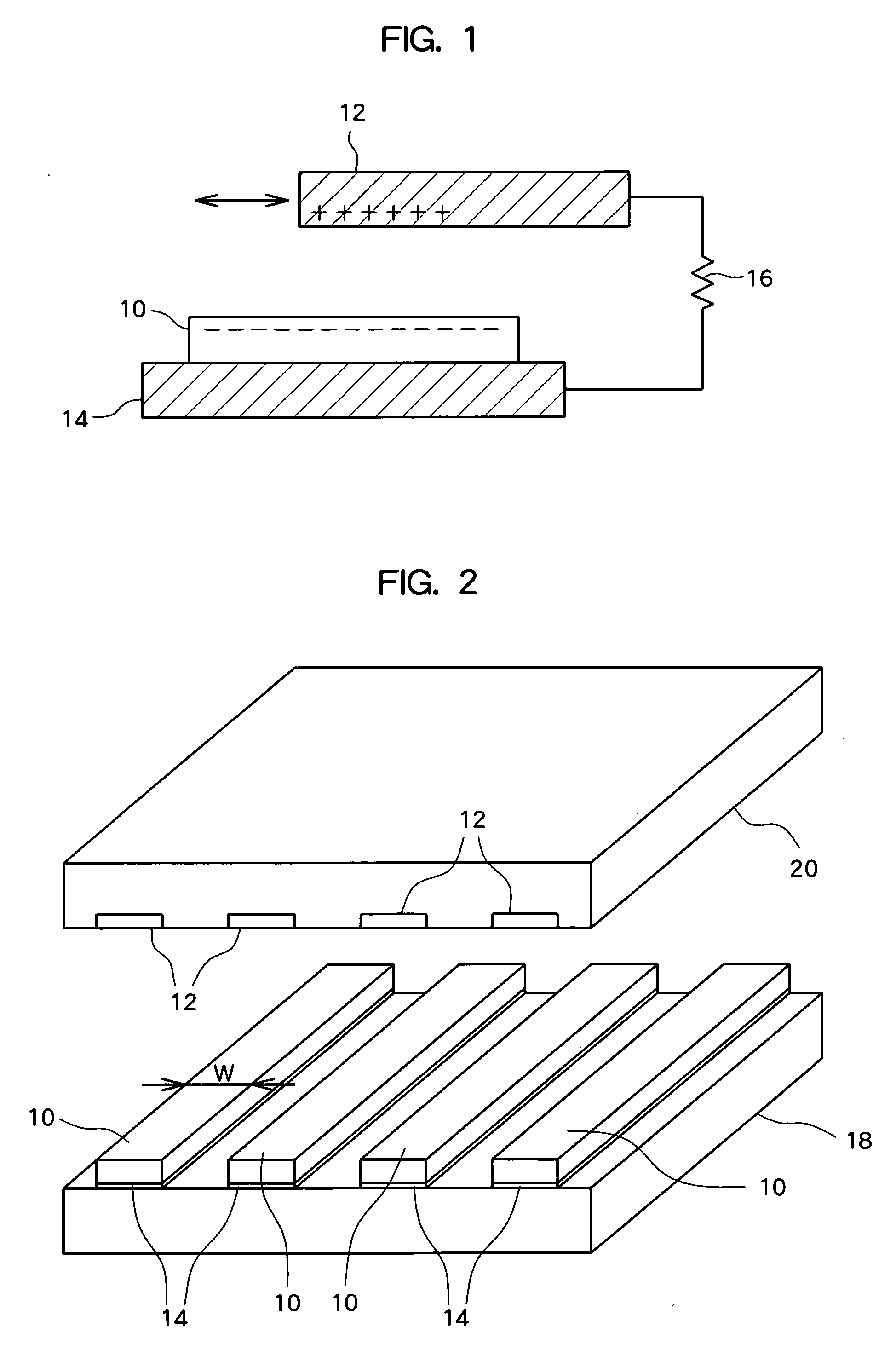
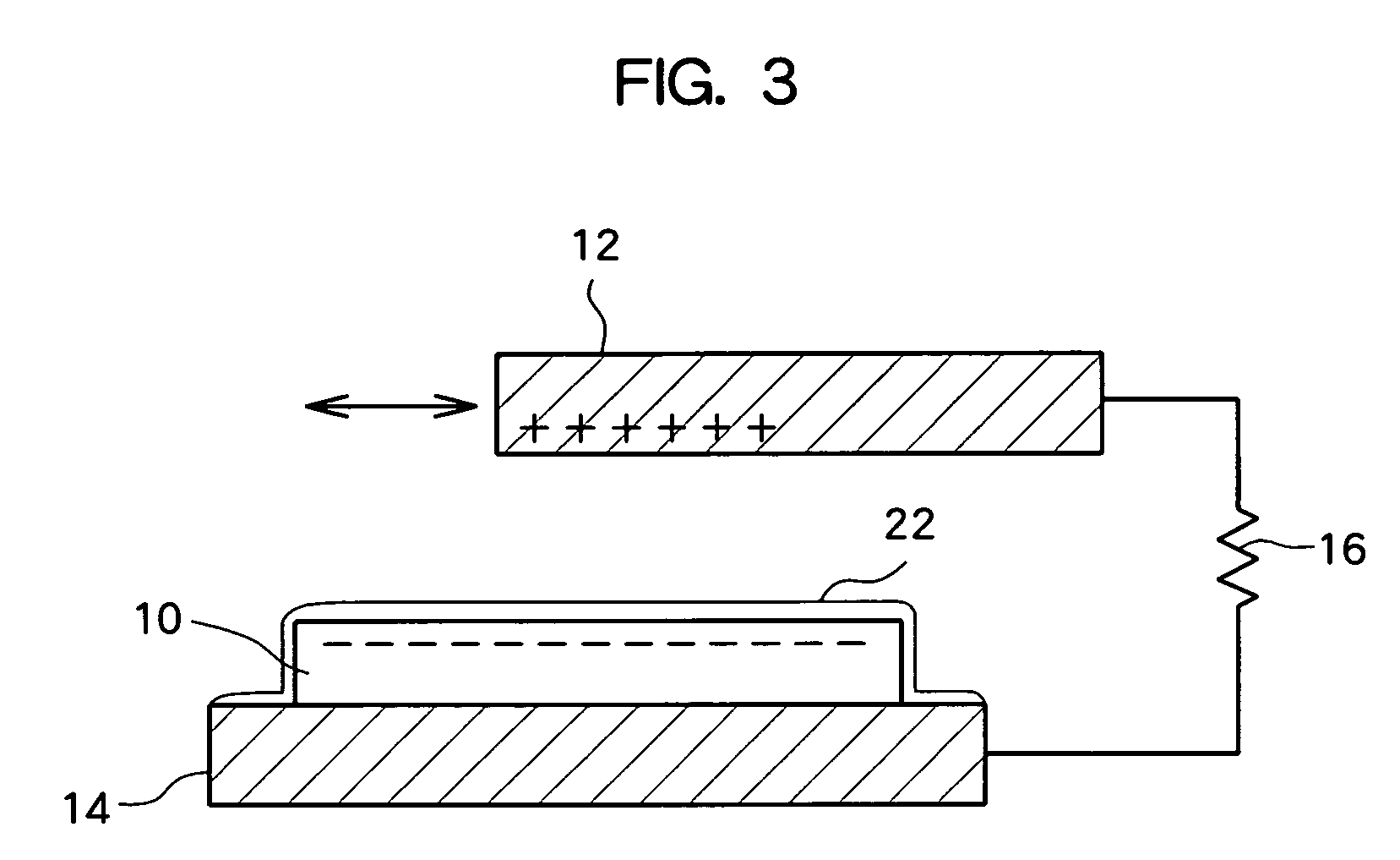
[0020]FIG. 1 is a sectional view of a structural example of an electrostatic induction conversion device according to embodiment 1 of the invention. In FIG. 1, an electret 10 formed by injecting an electric charge into the vicinity of the surface of an insulating material, is disposed between two conductors 12 and 14, and is constructed so that it can be moved relatively to at least the one conductor 12 opposite to the electret 10. Incidentally, as the injection of the electric charge into the electret 10, a well-known method such as liquid contact, corona discharge, electron beam, or back-lighted thyratron can be used.
[0021]The two conductors 12 and 14 are electrically connected to a load 16, and when the conductor 12 is moved, for example, in an arrow direction in the drawing, a positive electric charge is electrostatically induced in the conductor 12 by the electric charge (negative electric charge in FIG. 1) injected in the electret 10, and a current flows through the load 16. A...
example 1
[0037]Films with thicknesses of 3 μm and 15 μm were formed by spin coating using CYTOP (registered trademark) CTL-809M made by Asahi Glass Co., Ltd., and the surface charge density was measured after an electric charge was injected by corona discharge. Besides, as a comparison example, although Teflon (registered trademark) AF (Teflon AF 1601S) was used, since formation of a thick film was difficult, a film with a thickness of 3 μm was formed. The surface charge density was measured after the electric charge was injected by corona discharge, and the comparison with the film of CYTOP (registered trademark) with a thickness of 3 μm was performed.
[0038]Specifically, a charging condition was as follows: As a needle of the corona discharge, a stainless steel needle with an outer diameter of 0.7 mm and a tip angle of about 15 degrees was used, a DC high voltage power source (HAR-20R5 made by Matsusada Precision Inc.) was used to perform discharge for a predetermined time and at a predeter...
example 2
[0047]A film with a thickness of 20 μm was formed by spin coating using CYTOP (registered trademark) CTL-809M made by Asahi Glass Co., Ltd., and an electron was injected by corona discharge, so that an electret with a surface charge density of 0.93 mC / m2 and a surface potential of 1000 V was formed. Ten such electrets each having a strip shape of 1 mm×20 mm were formed. Besides, ten conductors opposite to the electrets and each having a strip shape of 1 mm×20 mm were formed, and the area was made 10 mm×20 mm. The conductor was horizontally vibrated at 10 Hz with 1 mm, so that a maximum electric output of 6 microwatts was obtained.
PUM
| Property | Measurement | Unit |
|---|---|---|
| thickness | aaaaa | aaaaa |
| width | aaaaa | aaaaa |
| specific dielectric constant | aaaaa | aaaaa |
Abstract
Description
Claims
Application Information


