Method for manufacturing thin film integrated circuit, and element substrate

a technology of integrated circuits and elements, applied in the direction of electrical apparatus, semiconductor devices, semiconductor/solid-state device details, etc., can solve the problems of complicated manufacturing process of extremely thin ic chips, and achieve the effect of short manufacturing time, simple and easy manufacturing, and short manufacturing tim

Inactive Publication Date: 2008-11-18
SEMICON ENERGY LAB CO LTD
View PDF15 Cites 71 Cited by
  • Summary
  • Abstract
  • Description
  • Claims
  • Application Information

AI Technical Summary

Benefits of technology

[0009]It is an object of the invention to provide a structure and a simple and easy process which enable production at a much lower cost.
[0011]An extremely thin IDF chip can be manufactured by separating an insulating substrate. After separated from the insulating substrate, the IDF chip may be transferred to a transposition substrate. The transposition substrate at this time is preferably a substrate having flexibility (hereinafter also referred to as a flexible substrate). In some cases, transferring an element of an IDF chip (including one in process of manufacturing) to another substrate as described above is referred to as “transfer”. The flexible substrate is often inexpensive, and reduction in cost of the IDF chip can be achieved. In addition, the insulating substrate can be reused. Therefore, further reduction in cost of the IDF chip can be achieved.
[0022]Since an etching rate of the metal film or the reactant having metal is high, the IDF chip can be manufactured in a short time in the invention. Further, a physical means in addition to a chemical means of etching the metal film or the reactant having metal can be used in the invention. Thus, the IDF chip can be manufactured more simply and easily and in a short time. The insulating substrate can be removed and an IDF chip can be transposed to an inexpensive flexible substrate, and the insulating substrate can be reused. Therefore, the IDF chip can be manufactured at a low cost.
[0023]According to the invention, IDF chips can be manufactured without being separated from each other. Consequently, there is no concern that an exhaust system of an apparatus is clogged with IDF chips during manufacturing. The complexity of handling extremely small IDF chips can be reduced. A thin IDF chip formed over a large substrate might warp due to stress. However, the warpage can be prevented since IDF chips can be manufactured to be connected with each other. A method which provides a connection region between the IDF chips can enhance warpage prevention effect. As described above, the invention can provide a simple and easy method for manufacturing an IDF chip.

Problems solved by technology

Handling of an extremely thin IC chip is complicated in a manufacturing process.

Method used


Image

  • Method for manufacturing thin film integrated circuit, and element substrate
  • Method for manufacturing thin film integrated circuit, and element substrate
  • Method for manufacturing thin film integrated circuit, and element substrate

Examples


embodiments mode 1

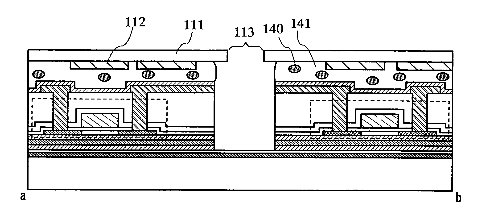
[0055]A mode of removing a metal film that is a separation layer and a reactant having the metal, after attaching an antenna substrate, is described in this embodiment mode.

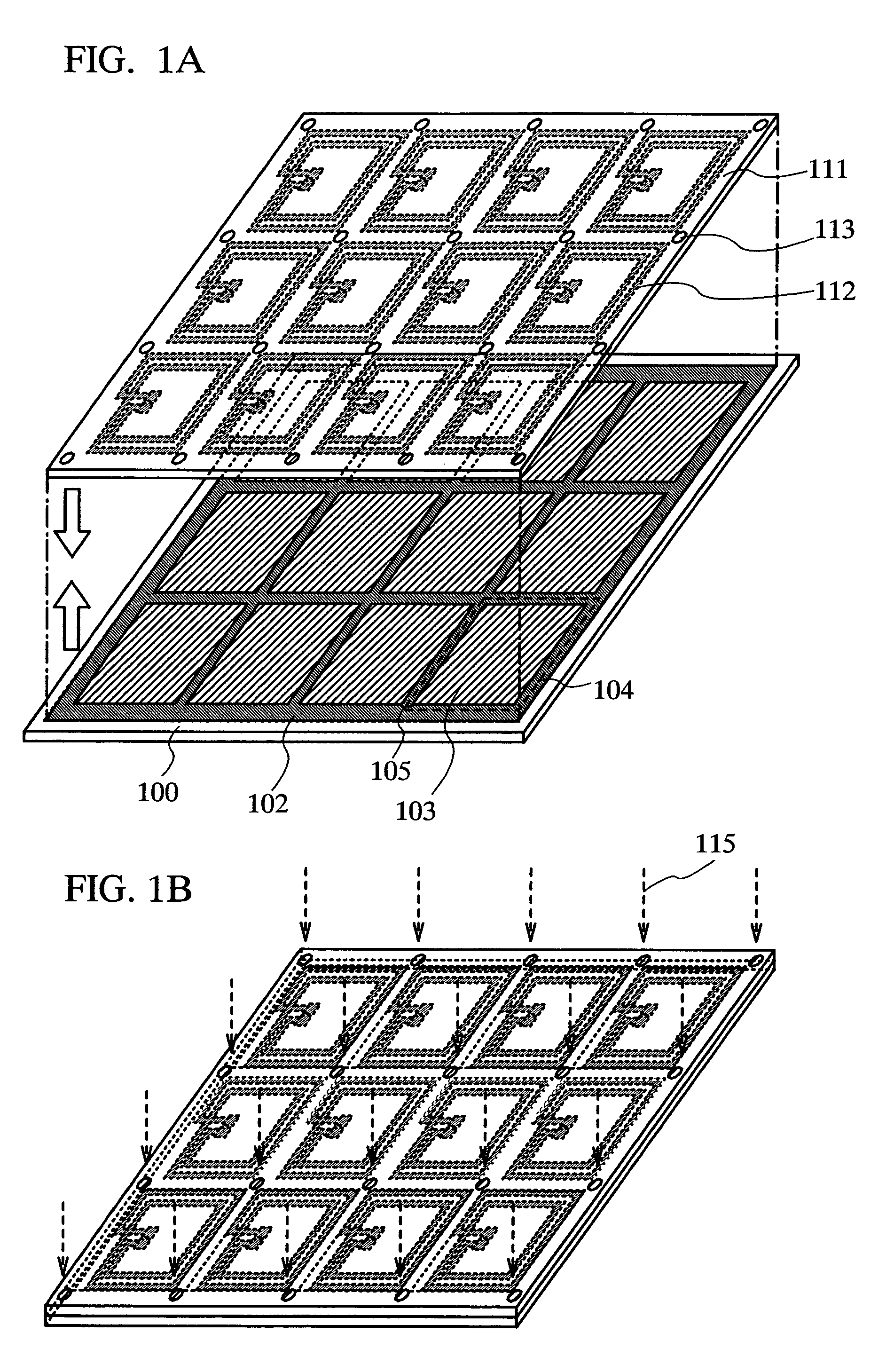
[0056]As shown in FIG. 1A, a metal film 102, and a thin film transistor (also referred to as a TFT) layer 103 having a semiconductor film as an active region are sequentially formed over an insulating substrate 100. Further, a reactant having the metal is formed over the metal film 102. A plurality of IDF chips 104 can be formed with the thin film transistor. Although a detailed structure of the TFT layer is to be described below, the semiconductor film is formed to be 0.2 μm or less, typically, 40 nm to 170 nm, and preferably, 50 nm to 150 nm in thickness.

[0057]Because of having an extremely thin semiconductor film as an active region, the IDF chip can be made thinner than a chip formed with a silicon wafer. A specific thickness of the IDF chip is 0.3 μm to 3 μm, typically, approximately 2 μm.

[0058]Then, a groov...

embodiments mode 2

[0085]A mode of selectively forming a groove and partially leaving an insulating film, a conductive film, or the like provided between IDF chips is described in this embodiment mode.

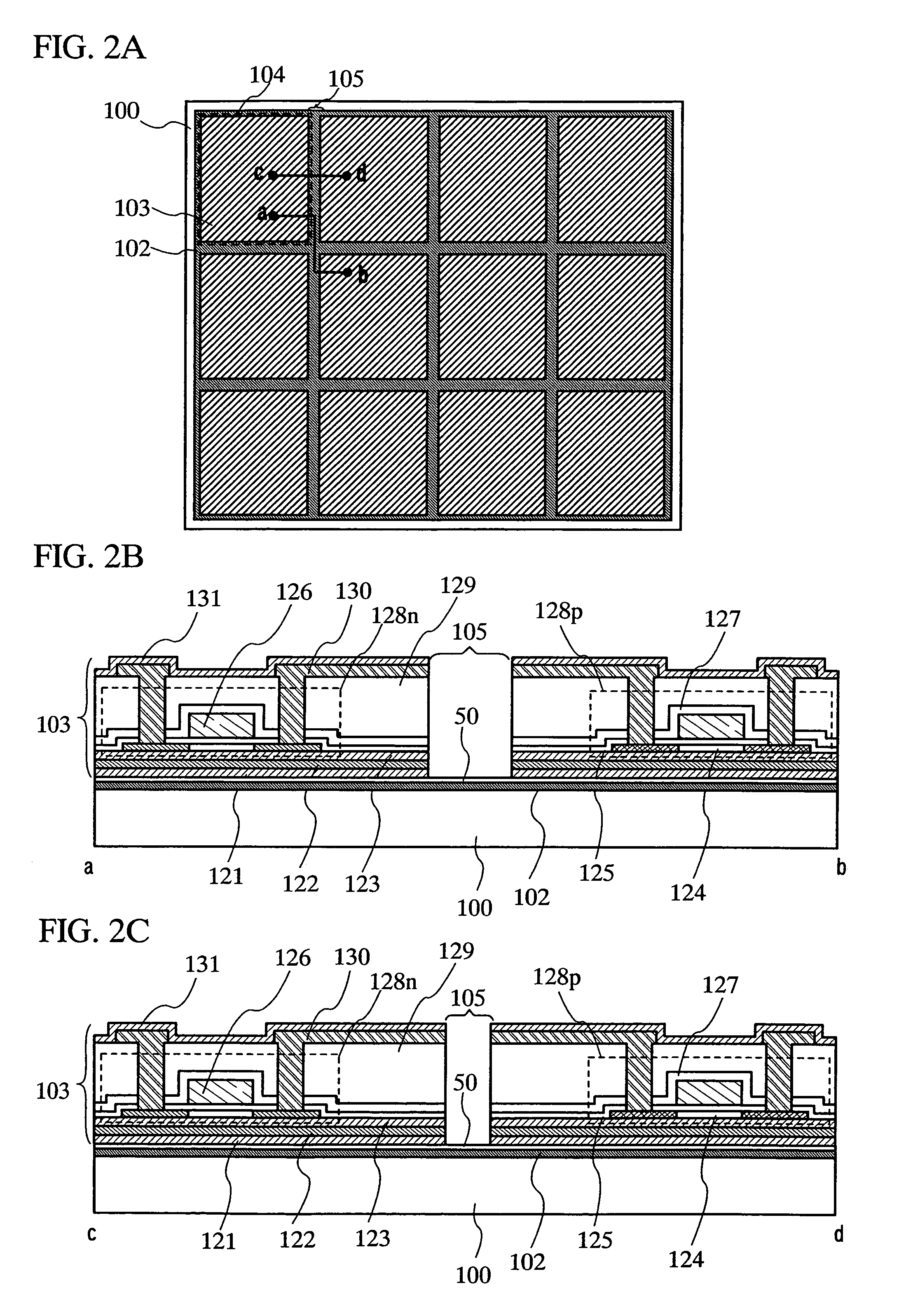
[0086]As shown in FIG. 8A, a metal film 102 as a separation layer, and a TFT layer 103 are sequentially formed over an insulating substrate 100, thereby forming a plurality of IDF chips 104 similarly as in Embodiment Mode 1. Further, as the separation layer, a reactant having the metal is formed over the metal film 102. Note that details of the TFT layer are to be described below.

[0087]Since a groove 105 formed at the boundary between the IDF chips is selectively formed, an insulating film, a conductive film, or the like is left at the boundary between the IDF chips. Such an insulating film, a conductive film, or the like at the boundary between the IDF chips is referred to as a connection region 106. Note that the connection region 106 may have a function of connecting the IDF chips to be connected and ...

embodiments mode 3

[0096]A method using a mode in which the antenna substrate which is provided with an opening, described in Embodiment Mode 1, is attached to the insulating substrate which is provided with a connection region at the boundary between IDF chips, described in Embodiment Mode 2, is described in this embodiment mode.

[0097]As shown in FIG. 20A, a metal film 102 as a separation layer, and a TFT layer 103 are sequentially formed over an insulating substrate 100. Further, as the separation layer, a reactant having the metal is formed over the metal film 102. A groove 105 is selectively formed to have a connection region 106 between IDF chips 104, as in Embodiment Mode 2.

[0098]Thereafter, an antenna substrate 111 provided with an antenna 112 and an opening 113 is attached as in Embodiment Mode 1. At this time, the antenna substrate is attached so as to position the opening 113 to the groove 105.

[0099]As shown in FIG. 20B, an etchant 115 is introduced into the opening and the groove. Then, the...


PUM

PropertyMeasurementUnit
thicknessaaaaaaaaaa
thicknessaaaaaaaaaa
thicknessaaaaaaaaaa

Abstract

Application form of and demand for an IC chip formed with a silicon wafer are expected to increase, and further reduction in cost is required. An object of the invention is to provide a structure of an IC chip and a process capable of producing at a lower cost. A feature of the invention is to use a metal film and a reactant having the metal film as a separation layer. An etching rate of the metal film or the reactant having metal is high, and a physical means in addition to a chemical means of etching the metal film or the reactant having metal can be used in the invention. Thus, the IDF chip can be manufactured more simply and easily in a short time.

Description

BACKGROUND OF THE INVENTION[0001]1. Field of the Invention[0002]The present invention relates to a method for manufacturing a thin film integrated circuit which can store much information and an element substrate in which the thin film integrated circuit is manufactured.[0003]2. Description of the Related Art[0004]In recent years, there has been an increasing need for a card with an IC chip or a tag with an IC chip capable of contactless data communication in all fields that require automatic identification, such as securities and management of goods. In consideration of application, it is required to manufacture such an IC card or an IC tag at a low cost since most IC cards or IC tags are to be thrown away after use. Cost reduction is required particularly for an IC chip formed with a silicon wafer.[0005]As an application of such an IC chip, an IC chip is put on a part of an animal and is used to control infectious diseases and to assure quality for safety management of livestock. ...

Claims


Application Information

Patent Timeline
Patent Type & Authority Patents(United States)
IPC IPC(8): H01L21/336H01L21/00H01L21/77H01L21/84H01L27/13H01L27/28H01L29/786H01R12/00
CPCH01L27/1214H01L27/1266H01L27/13H01L29/78603H01L27/28H01L2924/3511H01L27/1218H10K19/00H01L27/00
Inventor DOZEN, YOSHITAKATAMURA, TOMOKOTSURUME, TAKUYADAIRIKI, KOJI
Owner SEMICON ENERGY LAB CO LTD
Why Eureka
Try Eureka