MOS field effect transistor and manufacture method thereof

a field effect transistor and transistor technology, applied in the direction of basic electric elements, electrical apparatus, semiconductor devices, etc., can solve the problems of high substrate cost and high manufacture cost, increase the charge/discharge time of parasitic capacitors, and hinder the improvement of operation speed, so as to achieve fast operation and reduce power consumption

Inactive Publication Date: 2008-11-25
FUJITSU SEMICON LTD
View PDF3 Cites 0 Cited by
  • Summary
  • Abstract
  • Description
  • Claims
  • Application Information

AI Technical Summary

Benefits of technology

[0012]In view of the above problems, it is an object of the present invention to provide a method of manufacturing an MOS field effect transistor which achieves a faster operation and lower power consumption by using a thin film SOI structure.
[0013]It is another object of the present invention to provide an MOS field effect transistor, which is well matched with an existing process and is cost effective, without significantly changing the process steps, by using the manufacture method of the MOS field effect transistor.

Problems solved by technology

This leads to an increase in a pn junction capacitance of the source / drain regions and an increase in charge / discharge time of a parasitic capacitor, both of which hinder an improvement in the operation speed.
Since in the thin film SOI structure, an SOI substrate with a uniform SOI film thickness is prepared using complicated manufacture processes, it suffers a high substrate cost and a high manufacture cost.
In particular, a thin film SOI substrate of a complete depletion type which is expected to have a significant characteristic improvement becomes very expensive.
In the complete depletion type thin film SOI structure, a parasitic part and the channel become thinner, thus making it difficult to reduce the parasitic resistance.

Method used


Image

  • MOS field effect transistor and manufacture method thereof
  • MOS field effect transistor and manufacture method thereof
  • MOS field effect transistor and manufacture method thereof

Examples


embodiments

[0029]The present invention is further explained below with reference to embodiments, but the present invention is not limited to the embodiments.

first embodiment

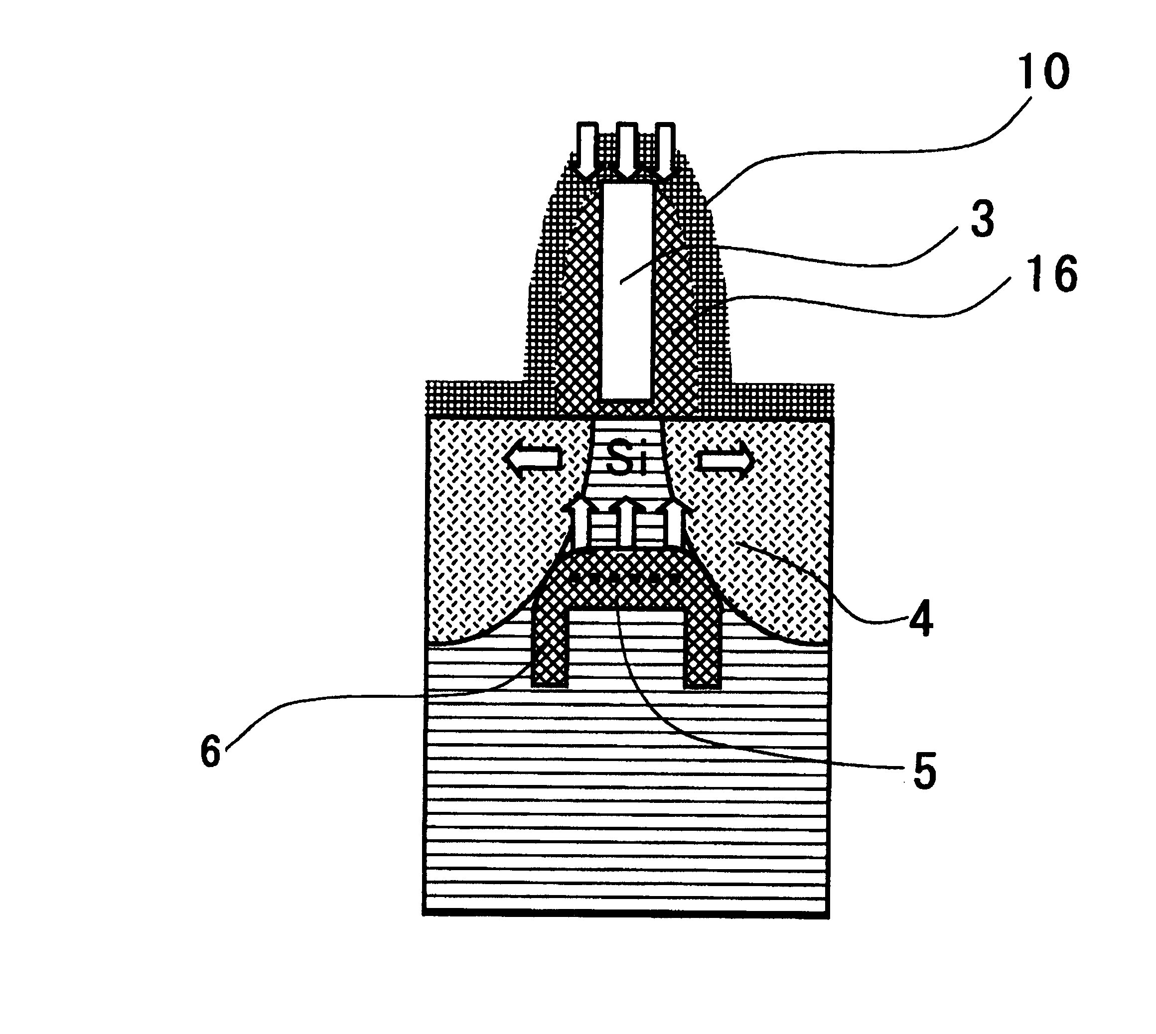
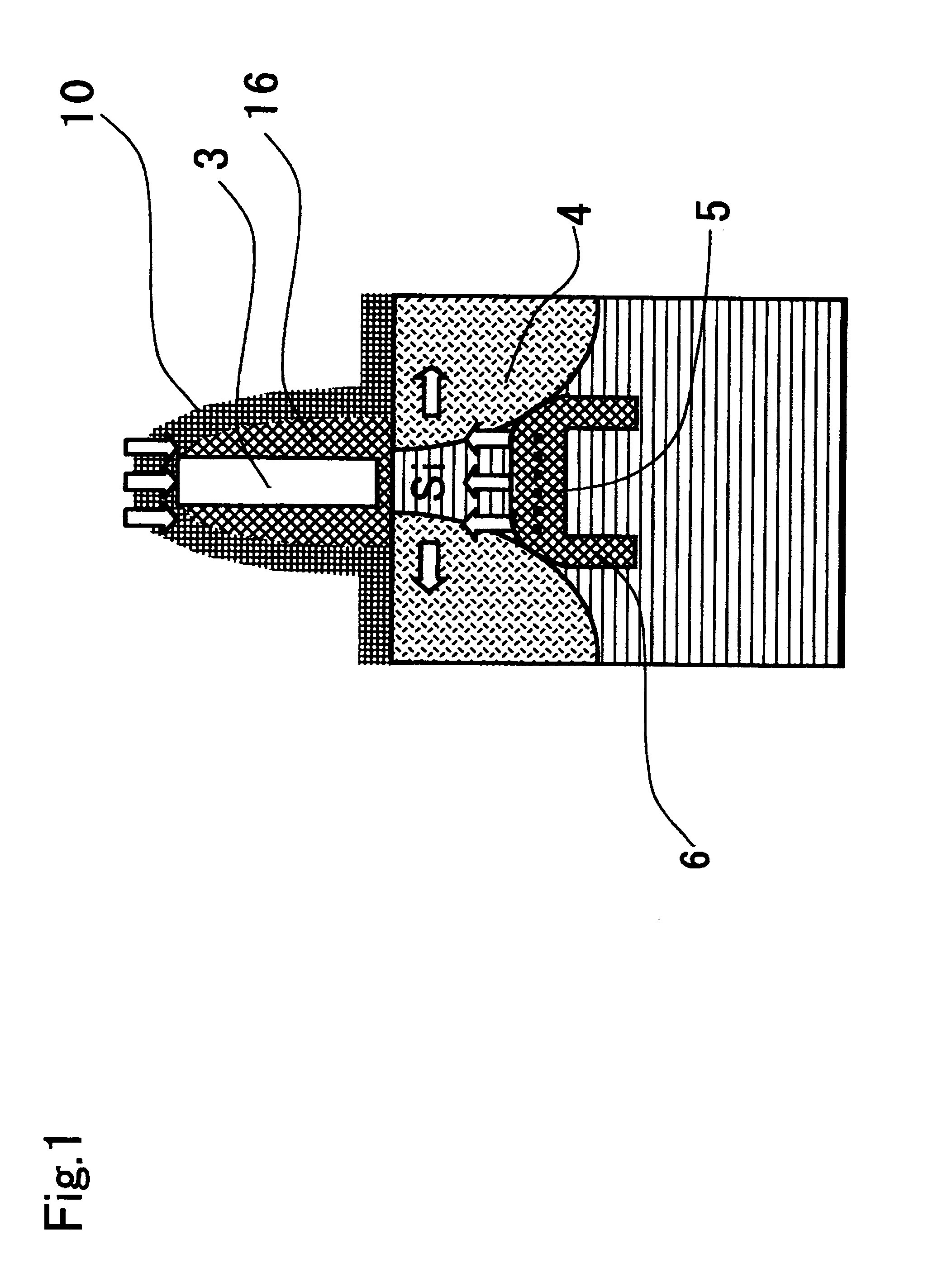
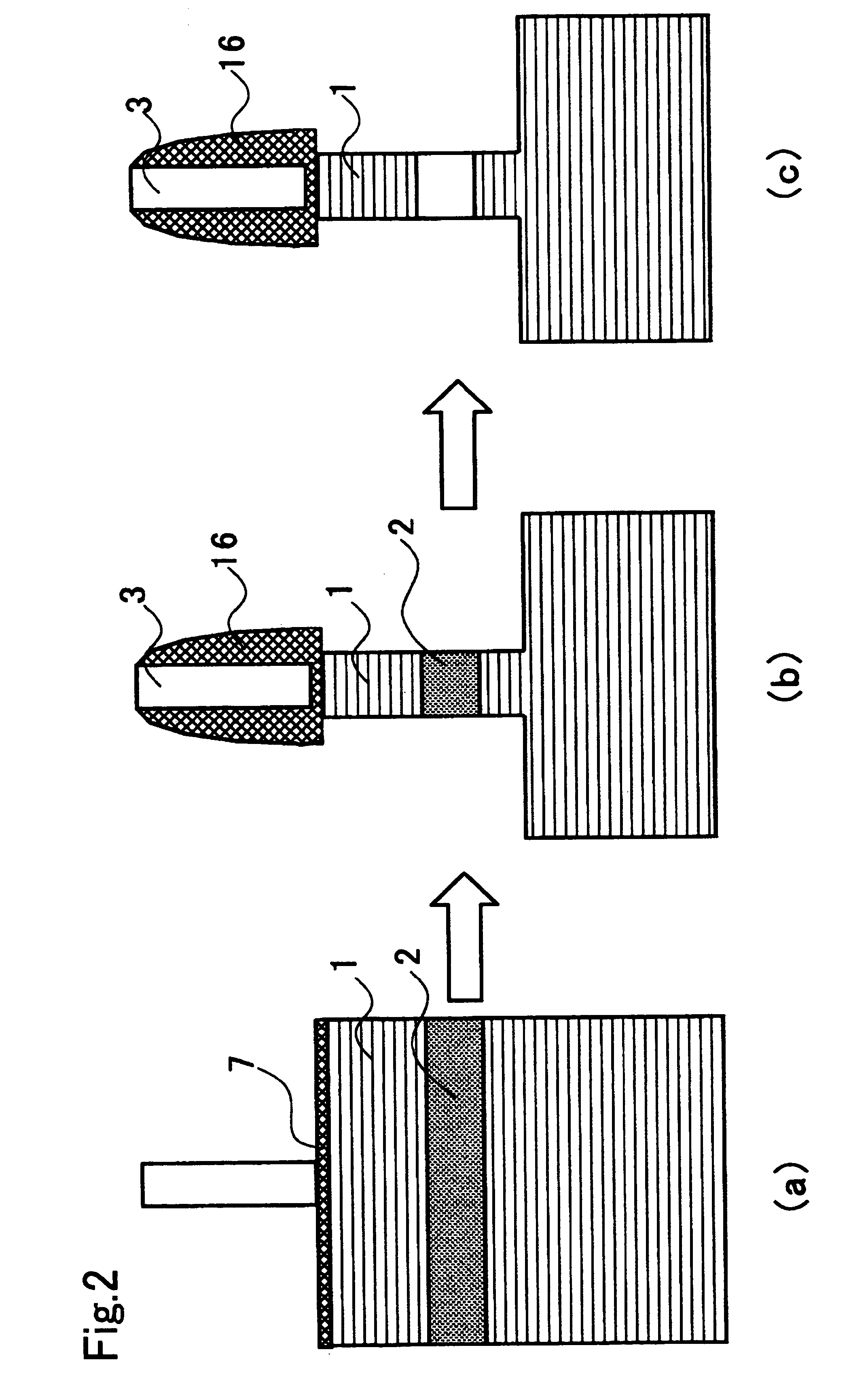
[0030]FIGS. 2A to 2C, FIGS. 3D to 3F, and FIGS. 4G and 4H are diagrams showing a manufacture process for an MOS field effect transistor according to a first embodiment. FIG. 2A shows a state in which a gate insulating film and a gate electrode are formed in the Si / SiGe lamination structure, FIG. 2B shows a state in which source / drain regions are etched, and FIG. 2C shows a state in which an Si / SiGe layer is removed. FIG. 3D shows a state in which a silicon oxide film is deposited, FIG. 3E shows a state in which a sidewall is formed, and FIG. 3F shows a state in which the source / drain regions are formed. FIG. 4G shows a state in which a contact etching stop film is formed, and FIG. 4H shows a state in which an interlayer insulating film is formed, a contact hole is formed therein, and an electrode is formed.

[0031]As shown in FIGS. 2A to 2C, after a device isolation step, the lamination of Si 1 and SiGe 2 is selectively formed at an active region, then a gate insulating film 7 of SiON...

second embodiment

[0036]FIGS. 5A to 5C, FIGS. 6D to 6F, and FIGS. 7G and 7H are diagrams showing a manufacture process for an MOS field effect transistor according to a second embodiment. FIG. 5A shows a state in which a gate insulating film and a gate electrode are formed in the Si / SiGe lamination structure, FIG. 5B shows a state in which source / drain regions are etched, and FIG. 5C shows a state in which an Si / SiGe layer is removed. FIG. 6D shows a state in which a silicon oxide film is deposited by a thermal oxidization step, FIG. 6E shows a state in which a sidewall is formed, and FIG. 6F shows a state in which the source / drain regions are formed. FIG. 7G shows a state in which a contact etching stop film is formed, and FIG. 7H shows a state in which an interlayer insulating film is formed, a contact hole is formed therein, and an electrode is formed.

[0037]As shown in FIGS. 5A to 5C, after a device isolation step, the lamination of Si 1 and SiGe 2 is selectively formed at an active region, and th...


PUM


Abstract

A method of manufacturing an MOS field effect transistor, which achieves a faster operation and lower power consumption by using a thin film SOI structure, is provided. The method of manufacturing an MOS field effect transistor to be formed on a semiconductor substrate having a channel layer on a buried oxide film, comprises the steps of forming: a gate electrode on the semiconductor substrate via a gate oxide film; forming a first sidewall which covers a side wall of the gate electrode; forming a box oxide film by etching the buried oxide film; and forming a second sidewall which covers a side wall of the box oxide film in such a way that the second sidewall extends downward along the side wall of the box oxide film.

Description

CROSS-REFERENCE TO RELATED APPLICATIONS[0001]This application is based upon and claims the benefit of priority from the prior Japanese Patent Application No. 2005-12508, filed on Jan. 20, 2005, the entire contents of which are incorporated herein by reference.BACKGROUND OF THE INVENTION[0002]1) Field of the Invention[0003]The present invention relates to an MOS (Metal Oxide Semiconductor) field effect transistor that has a thin film SOI (Silicon On Insulator) structure, and a method of manufacturing the MOS field effect transistor.[0004]2) Description of the Related Art[0005]For faster information processing and data communication and lower power consumption, there are demands for MOS field effect transistors with enhanced performances which ensures a faster operation with a low leak current. To enhance performances of the MOS field effect transistors at a low cost by miniaturization of the structure, however, the structure must be optimized in consideration of various elements.[000...

Claims


Application Information

Patent Timeline
Patent Type & Authority Patents(United States)
IPC IPC(8): H01L27/01H01L27/12H01L31/0392
CPCH01L29/66772H01L29/7842H01L29/78639H01L29/78654
Inventor SHIMA, MASASHI
Owner FUJITSU SEMICON LTD
Why Eureka
Try Eureka