Eureka AIR delivers breakthrough ideas for toughest innovation challenges, trusted by R&D personnel around the world.

Dual data rate memory strobe checker

Inactive Publication Date: 2008-11-25
HEWLETT-PACKARD ENTERPRISE DEV LP
View PDF4 Cites 27 Cited by
  • Summary
  • Abstract
  • Description
  • Claims
  • Application Information

AI Technical Summary

Benefits of technology

[0004]In one embodiment of the invention, a memory controller includes a gate circuit passing or blocking a data strobe signal from a memory device, a delay circuit delaying the data strobe signal from the gate circuit, a read buffer capturing values of a data signal from the memory device in response to the data strobe signal received from the delay circuit, a strobe counter incrementing a detected strobe count by the number of edges detected in the data strobe signal, and a

Problems solved by technology

Such inadvertent capture corrupts the data being read.
Missing strobe pulses can be caused by memory device failure where DQS data strobe signal is stuck in one state or is missing, or by software error that uses a nonexistent memory address.
When the memory controller is not expecting the data strobe signal from the memory device, the control logic compares the detected and the expected strobe counts and reports a strobe error when they do not match.

Method used


Image

  • Dual data rate memory strobe checker
  • Dual data rate memory strobe checker
  • Dual data rate memory strobe checker

Examples


Embodiment Construction

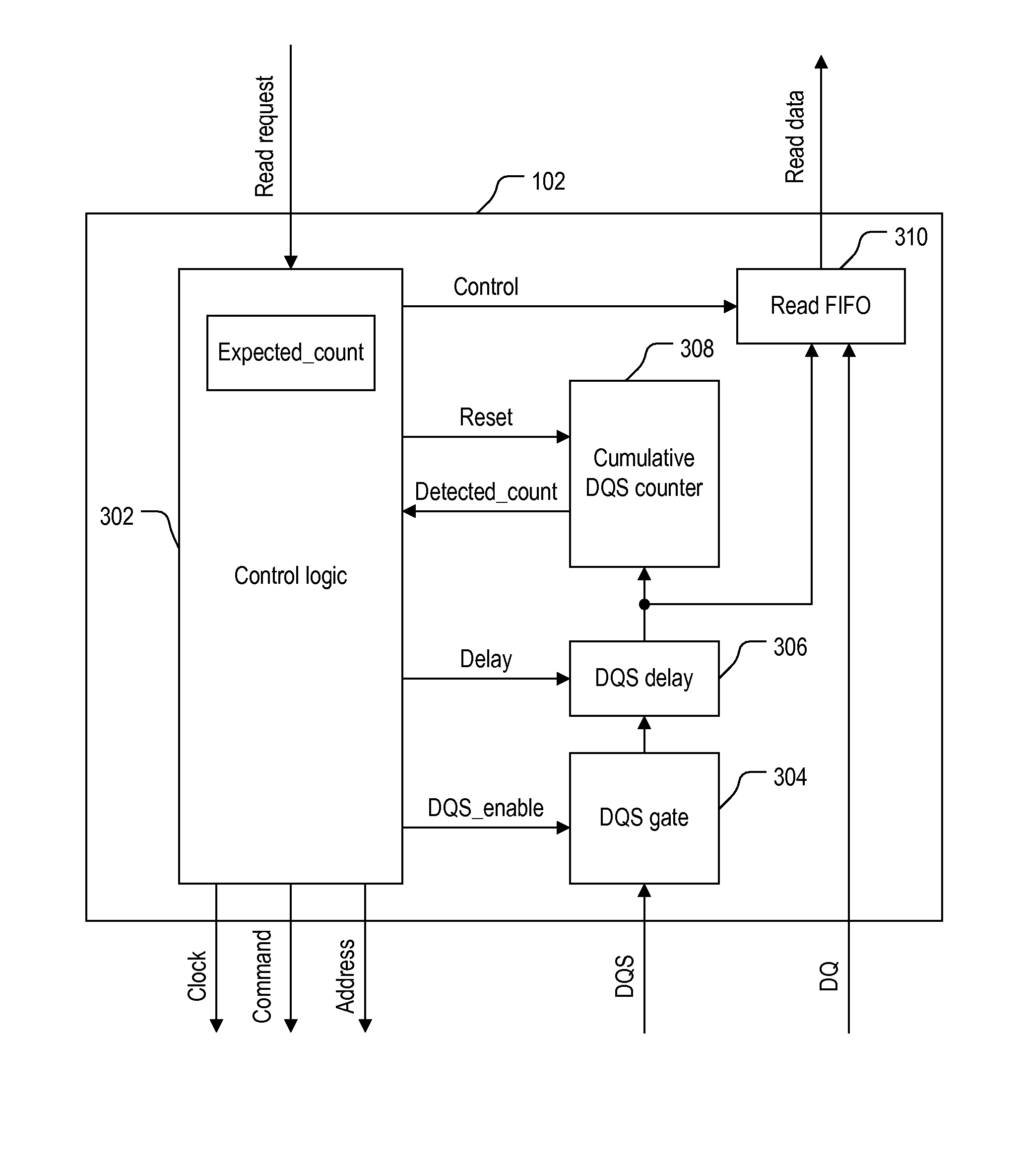
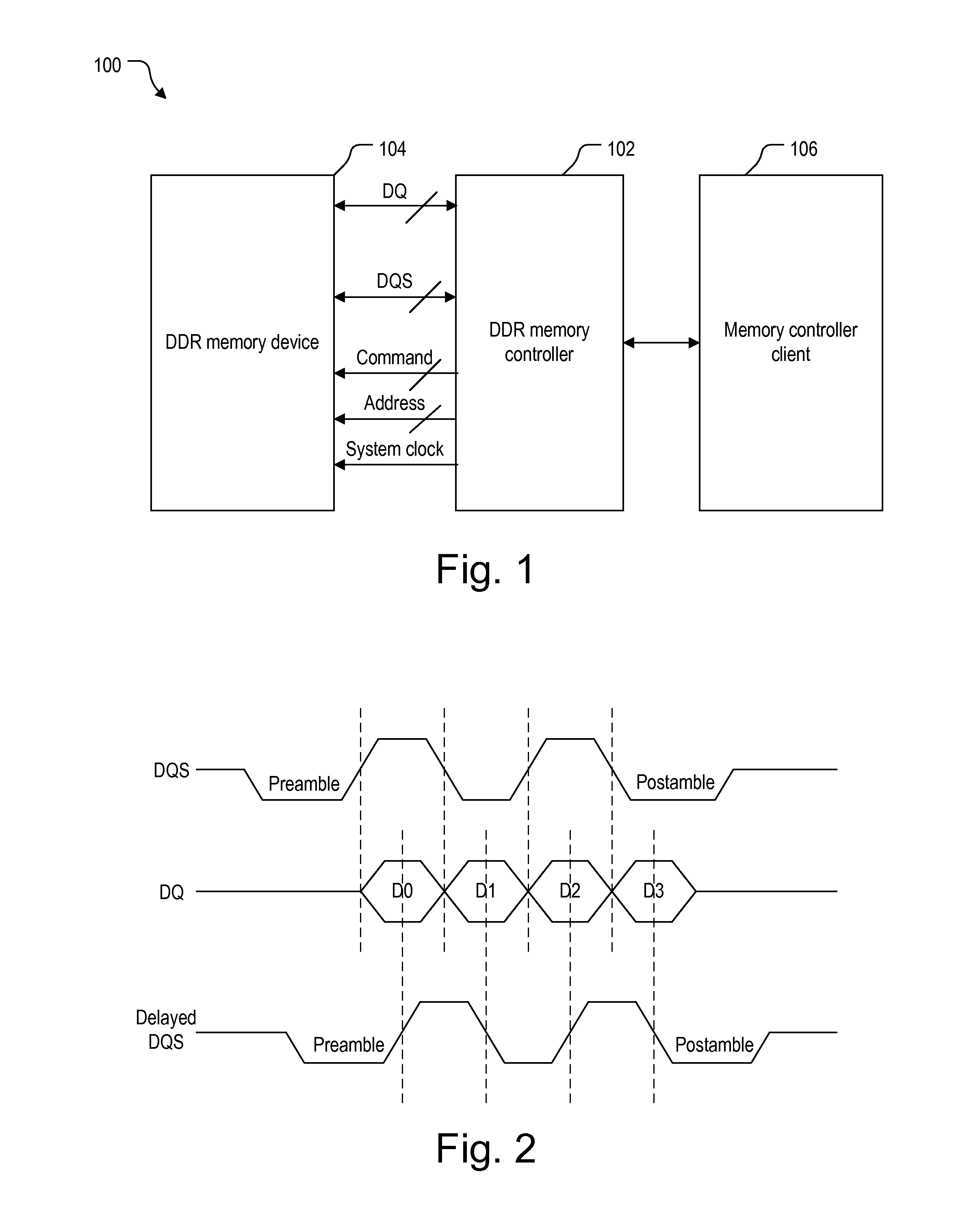
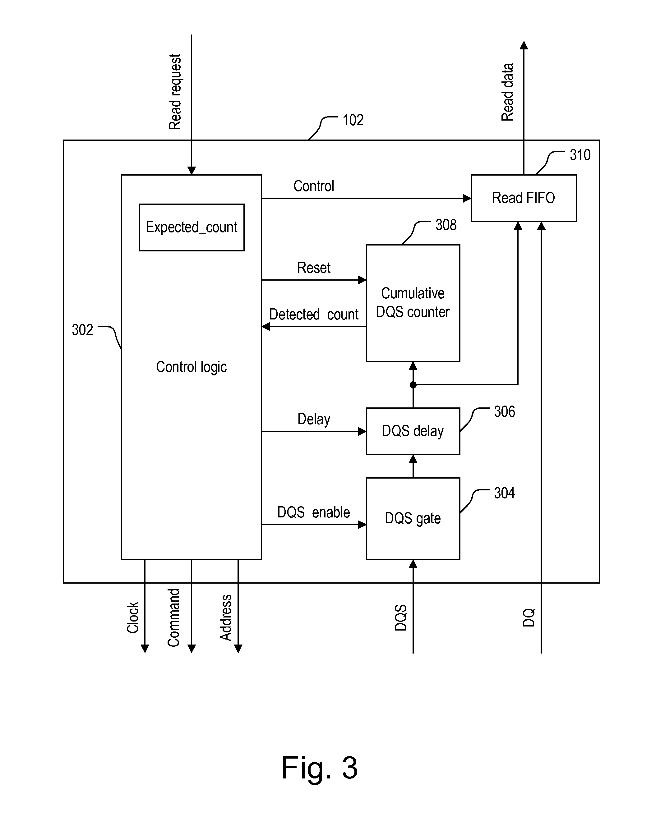
[0011]FIG. 1 is a block diagram of a data processing system 100 including a memory controller 102 coupled between a memory device 104 and a memory controller client 106 in one embodiment of the invention. Although only one memory device 104 is shown, memory controller 102 may be coupled to additional memory devices.

[0012]Memory controller 102 communicates with memory device 104 through a source synchronous interface while memory controller 102 communicates with memory controller client 106 through a synchronous interface with a system clock. In a read operation, memory controller 102 receives a read request from memory controller client 106 and then issues the appropriate read command and address to memory device 104. In response, memory device 104 returns data signals on DQ lines and a data strobe signal on a DQS line. For purposes of this disclosure, DQ and DQS are used to describe the signals and the lines on which the signals travel interchangeably.

[0013]In one embodiment, memor...


PUM


Abstract

A memory controller includes a gate circuit gating a data strobe signal from a memory device, a delay circuit delaying the data strobe signal from the gate circuit, a read buffer capturing values of a data signal from the memory device in response to the data strobe signal, a cumulative strobe counter incrementing a detected strobe count by the number of edges detected in the data strobe signal, and a control logic controlling the gate circuit and receiving the detected strobe count from the strobe counter. The control logic enables and disables the gate circuit after the start of a preamble and before the end of a postamble in the data strobe signal, respectively. When the memory controller is not expecting the data strobe signal from the memory device, the control logic compares the detected and the expected strobe counts and reports a strobe error when they do not match.

Description

FIELD OF INVENTION[0001]This invention relates to a memory controller for dual data rate (DDR) memory devices.DESCRIPTION OF RELATED ART[0002]In a typically single data rate (SDR) system, both the memory controller and the memory device (e.g., a synchronous dynamic random access memory) transmit and capture data in response to a single system clock. In a DDR system, the memory device outputs both a data signal DQ and a data strobe signal DQS that are edge-aligned with each other to the memory controller. The memory controller shifts data strobe signal DQS to center it with data signal DQ and then uses rising and falling edges of data strobe signal DQS to capture the values of data signal DQ. A preamble in data strobe signal DQS indicates the start of data transmission and a postamble in data strobe signal DQS indicates the end of the data transmission.[0003]An unintentional transition in the data strobe signal DQS, often referred to as a “glitch,” may be interpreted by the memory co...

Claims


Application Information

Patent Timeline
IPC IPC(8): G11C7/00
CPCG06F13/1689
Inventor GRIFFITH, DAVID L.CEKLEOV, MICHEL P.
Owner HEWLETT-PACKARD ENTERPRISE DEV LP
Why Eureka
Eureka Blog
Learn More