Dissociated fabrication of packages and chips of integrated circuits

a technology of integrated circuits and fabrication methods, applied in the direction of electrical equipment, semiconductor devices, semiconductor/solid-state device details, etc., can solve the problems of significant limitations in the application of processing technologies and materials for packaging, and the limited range of applicable processing methods, so as to reduce the thermal induced mechanical stress of the package

Inactive Publication Date: 2008-12-02
POLARIS INNOVATIONS LTD
View PDF18 Cites 0 Cited by
  • Summary
  • Abstract
  • Description
  • Claims
  • Application Information

AI Technical Summary

Benefits of technology

[0008]In one aspect, the present invention is directed to decrease the temperature load on fabrication of semiconductor chips by dissociated fabrication of packages and chips. Most parts of the package are fabricated separately from the chip. This allows a higher freedom for processing temperatures and materials regarding package fabrication.
[0011]Another aspect of the invention is to minimize the thermal induced mechanical stress of the package. For that, the semiconductor chips in the frame have no fast contact with the inside of the frame and are held only by the bond contacts of the metal strips with the bond pads on the chip. Since the chips have many degrees of freedom, thermal expansion of the chip will not lead to any mechanical stress.

Problems solved by technology

Most memory chips must not be exposed to temperatures above 200° C. because of so called retention failures.
The result is that the applicable processing technologies and materials for packaging are limited significantly.
However, future and some currently available memory products, especially stacked chips require a different packaging method to meet desired performance, cost and reliability.
As mentioned before the applicable processing methods are then limited to temperatures below 200° C.

Method used


Image

  • Dissociated fabrication of packages and chips of integrated circuits
  • Dissociated fabrication of packages and chips of integrated circuits
  • Dissociated fabrication of packages and chips of integrated circuits

Examples


Embodiment Construction

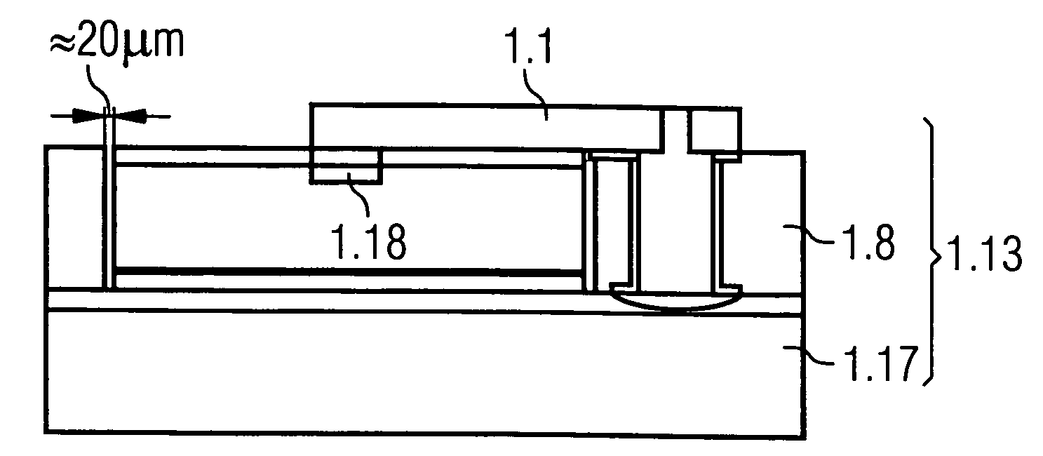
[0020]The dissociated fabrication and final package of chips of integrated circuits describes completely prefabricated semiconductor chips surrounded by a frame and held in it by electrical and mechanical connections between bond pads on the chip in a central row arrangement and metal traces on the frame terminate in a semiconductor module. This semiconductor module can be stacked in a stacked arrangement.

[0021]To realize such semiconductor modules and stacked arrangement of them with a dissociated fabrication of the components will be described hereinafter.

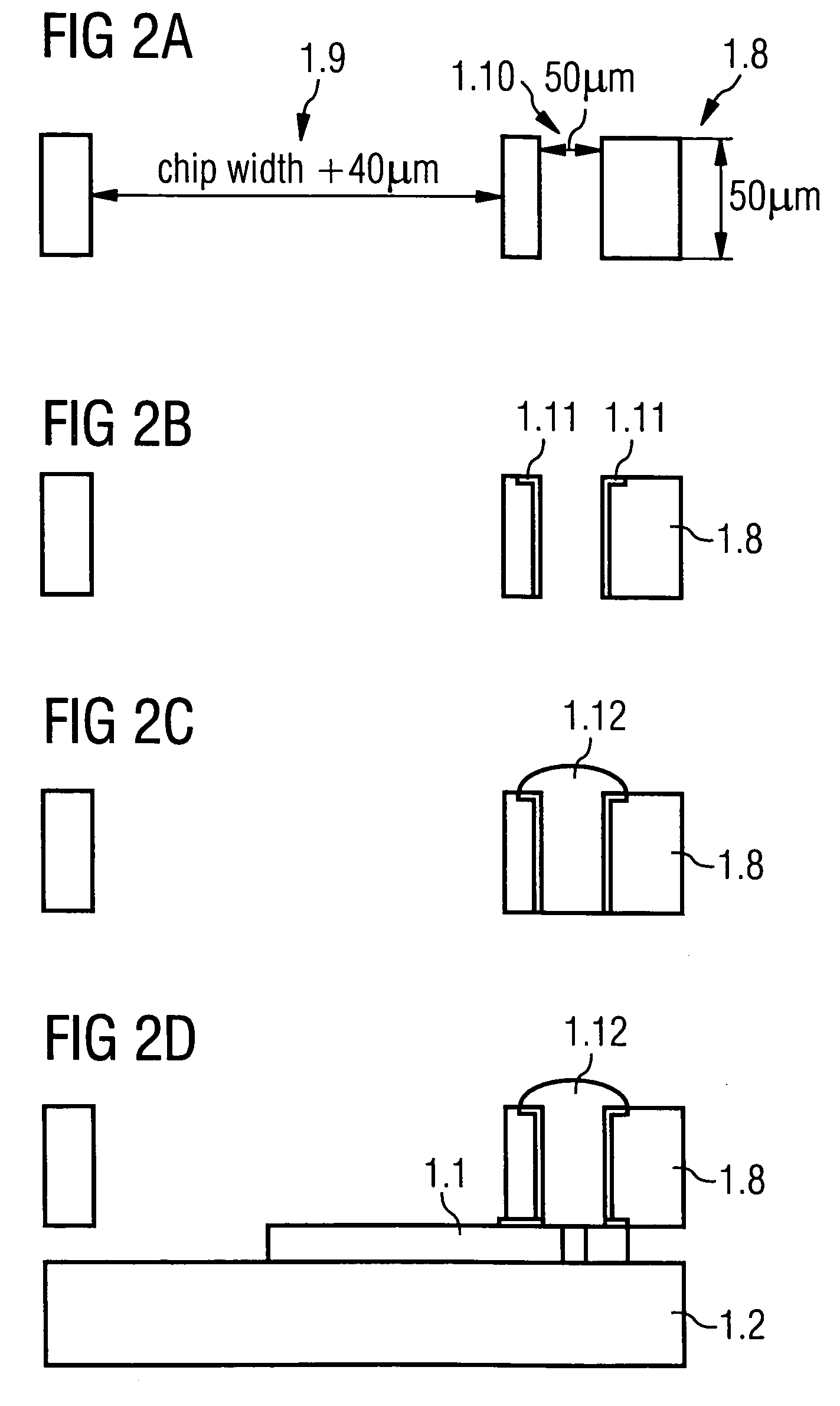
[0022]A first example will describe a simplified process for fabricating the necessary components of a semiconductor module and finally a stacked arrangement of such modules.

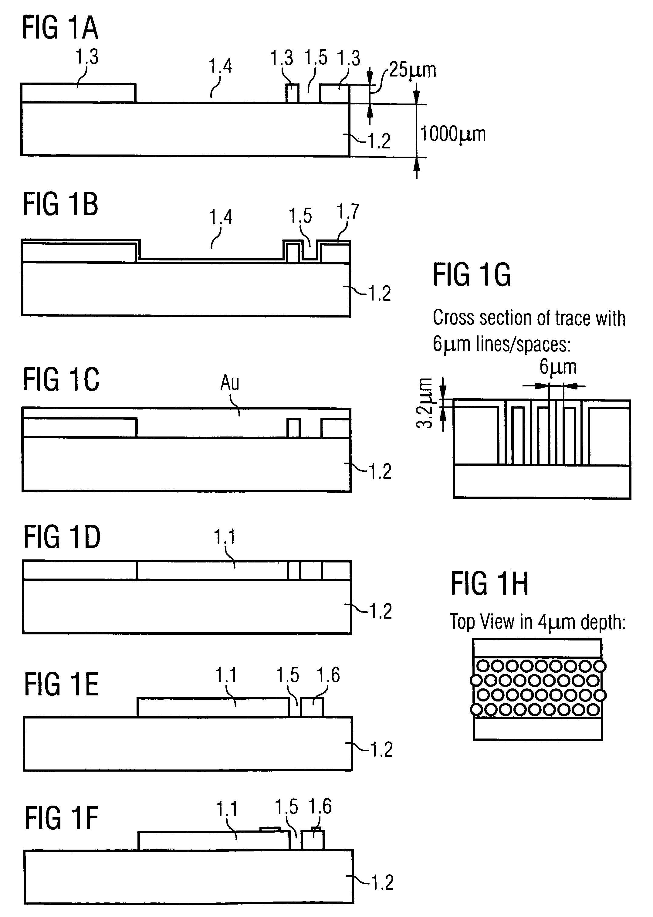
[0023]FIGS. 1A to 1F depict a first level processing to realize metal traces 1.1, shown is a schematic cross section (see e.g., FIG. 1D). In the preferred embodiment, a number of metal traces 1.1 are arranged side by side with a lateral distance of e.g., 6 μm...


PUM


Abstract

A method of fabricating a semiconductor component includes providing a prefabricated frame that includes metal traces and lead-through contacts. A semiconductor chip is mounted into the prefabricated frame such that the semiconductor chip is embedded within a rim of the prefabricated frame. Contact regions on a surface of the semiconductor chip are electrically connected with the metal traces of the prefabricated frame such that the contact regions are electrically coupled to the lead-through contacts via the metal traces.

Description

TECHNICAL FIELD[0001]The invention is concerned with a dissociated fabrication and final package of chips of integrated circuits with so called “redistribution layers” or metal traces.BACKGROUND[0002]It is well known for one skilled in the art that the fabrication of integrated circuits requires many fabrication steps, starting with structuring a silicon chip for the desired electrical function, e.g., a memory chip or a processor. This process covers deposition steps, photolithography steps, etching steps and other fabrication steps until the desired function is performed. After that, the integrated circuit is finally mounted on a substrate, such as a printed circuit board, and the electrical interconnections between the circuit and the board are carried out at the same time.[0003]This electrical interconnection is often established by wiring or wire bonding. In a final step, the integrated circuit must be provided with a housing, which can be formed by molding a suitable mold compo...

Claims


Application Information

Patent Timeline
Patent Type & Authority Patents(United States)
IPC IPC(8): H01L21/00
CPCH01L21/6835H01L23/13H01L24/24H01L24/82H01L24/96H01L25/105H01L2221/68309H01L2221/68331H01L2221/68359H01L2224/24145H01L2224/82001H01L2225/06541H01L2225/06551H01L2225/06555H01L2225/06572H01L2924/01005H01L2924/01013H01L2924/01029H01L2924/01079H01L2924/01082H01L2924/04953H01L2924/14H01L2924/01006H01L2924/01024H01L2924/01033H01L2924/01072H01L2924/014H01L2225/1058H01L2924/10253H01L2924/00H01L2924/181
Inventor GROSS, HARALD
Owner POLARIS INNOVATIONS LTD
Why Eureka
Try Eureka