Method for manufacturing display element

a technology of display elements and manufacturing methods, applied in the field of display elements, can solve the problems increasing the number of manufacturing processes, reducing the efficiency of the system, etc., and achieving the effect of reducing display quality

Inactive Publication Date: 2008-12-16
E INK CORPORATION
View PDF28 Cites 6 Cited by
  • Summary
  • Abstract
  • Description
  • Claims
  • Application Information

AI Technical Summary

Benefits of technology

[0018]The present invention has been achieved in the light of the above-mentioned problems. It is an object of the invention to provide a display element and a manufacturing method therefor in which degradation in display quality due to remaining air bubbles caused at a time of bonding a substrate on a display layer of binder dispersion type is prevented in.
[0021]With this invention, since one or more display function layers other than the display layer are formed on the display layer, the display function layers on the display layer act as the flattening layers for flattening the roughness on the surface of the display layer to decrease the roughness on the bonded face and prevent air bubbles from being mixed. Thereby, the reflection of light due to bubbles having different refractive index is suppressed, so that the display contrast ratio is not decreased or the image noise is relieved to enhance the display quality.
[0022]The air bubbles cause a variation in divided voltage on the display layer, and may be observed as uneven display, when the voltage is applied to the display layer. Therefore, remaining bubbles on the bonded face between the display function layer formed on the display layer and the second substrate are desirably reduced to the least. From this viewpoint, an adhesive layer may be provided on this bonded face. This adhesive layer fills up the roughness on the bonded face to reduce the remaining bubbles and prevent the reflection of light due to bubbles. Also, the adhesive layer not only reduces the remaining bubbles but also fills up the roughness of the display layer, with the action of reducing a variation in the divided voltage. This is because the variation in the divided voltage is reduced with the greater dielectric constant of the dielectric substance (here, bubbles and the adhesive layer) inserted in series, and the dielectric constant of the adhesive constituting the adhesive layer is usually three or more, which is above the dielectric constant (=1) of bubbles. Moreover, since another display function layer is formed on the display layer to decrease the roughness, the film thickness of the adhesive layer is smaller, making it possible to suppress the increase in the driving voltage to the minimum.
[0023]The display function layer formed on the display layer may be the light shielding layer. By forming the light shielding layer on the display layer, the light shielding layer and the display layer are intimately contacted to prevent the bubbles from remaining on the surface of the display layer. Though bubbles may remain between the light shielding layer and the second substrate, the bubbles are hidden under the light shielding layer as seen from the observer, who can not observe the scattered light due to bubbles. Therefore, it is possible to prevent the degradation in the display quality from being caused by the bubbles. Also, the light shielding layer acts as the flattening layer for flattening the roughness on the surface of the display layer, thereby decreasing the roughness on the bonded face and preventing the bubbles from being mixed.
[0024]The light shielding layer is formed at high productivity by coating an aqueous coating agent with the black coloring matter dispersed or dissolved in the binder solution. Typically, the display material is often subject to physical or chemical damages from the solvent of binder resin, whereby the selection of the solvent or dispersion medium is important. As a result of examining various solvents, it has been found that the use of an aqueous coating agent containing at least 50% or more of water is effective to reduce the damages.

Problems solved by technology

For example, it takes several to several tens hours to make a filling process of the liquid crystal material in the liquid crystal display element, leading to a main cause of impeding the productivity.
Therefore, there has been a problem that number of members and number of manufacturing processes are increased to raise the cost.
The remaining bubbles reflect light to lower the display contrast ratio and / or to increase the image noise, resulting in a problem that the display quality is degraded.
However, if the mixture ratio of binder is increased, the voltage (driving voltage) required for the display is caused to increase.
Also, even if the particle diameter of display material is smaller, there is a limitation in relieving the roughness.
However, considerable film thickness is required to provide the flattening layer.
Although there is an effect for relieving the roughness, there is a problem of increasing the driving voltage as with the case where the mixture ratio of binder is increased.

Method used


Image

  • Method for manufacturing display element
  • Method for manufacturing display element
  • Method for manufacturing display element

Examples


first embodiment

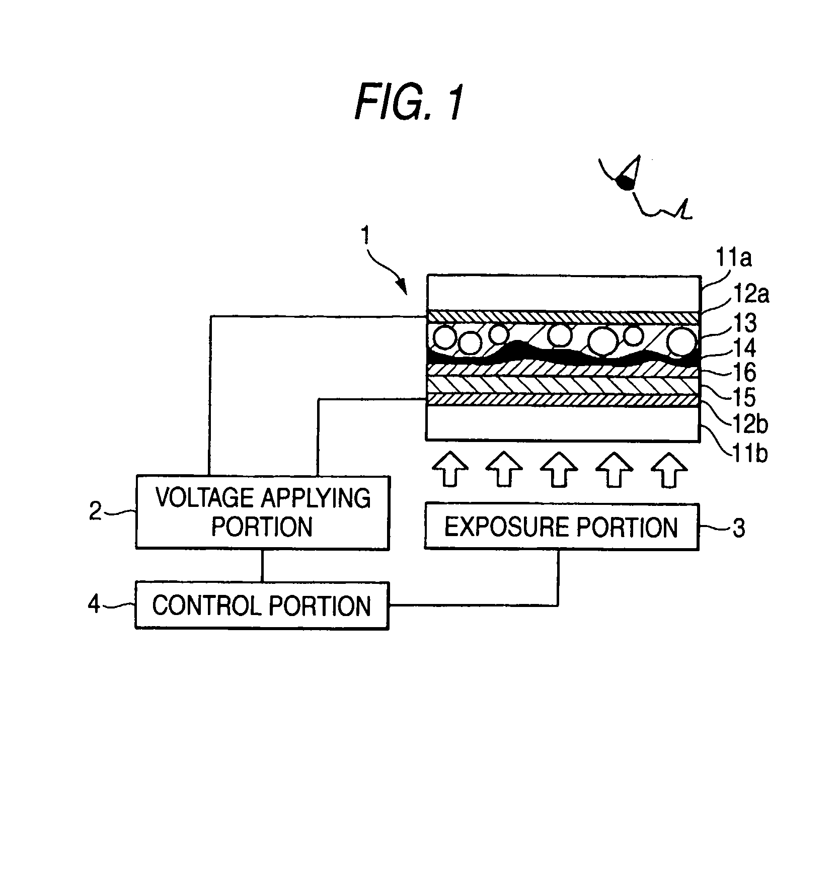
[0036]FIG. 1 is a cross-sectional view showing a display element according to a first embodiment of the present invention. In FIG. 1, the same or like parts are designated by the same numerals as in FIG. 9, and the duplicate description maybe omitted. Reference numeral 16 denotes an adhesive layer. In this embodiment, a display element of optically writing type using a cholesteric liquid crystal is described as one example of the display element.

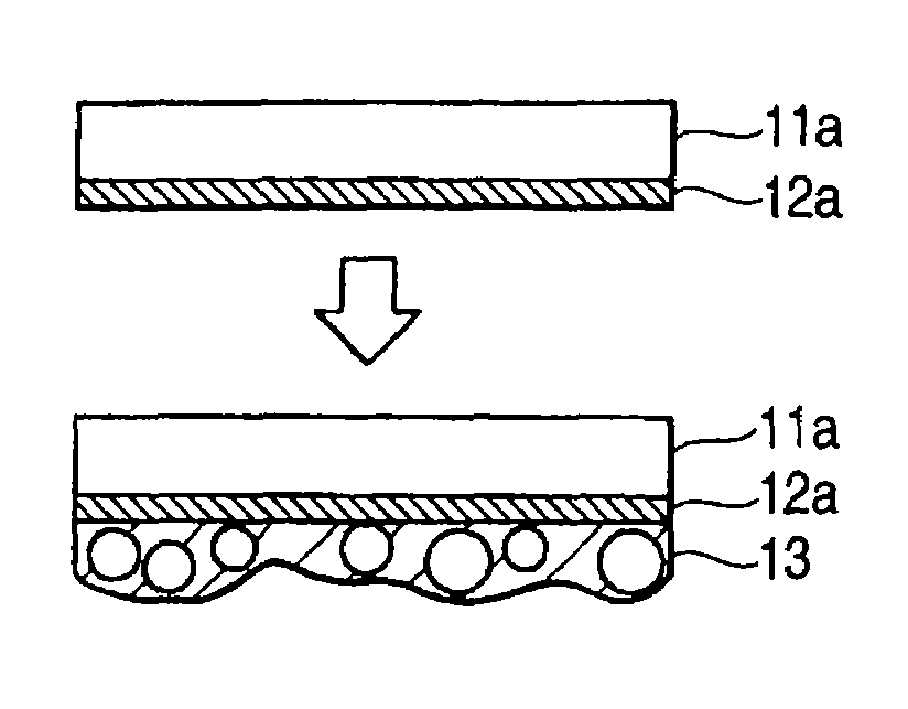
[0037]The display element 1 has a plurality of display function layers carried by a pair of substrates 11a and 11b to implement the display function. In this example, an electrode 12a, a display layer 13, a light shielding layer 14, an adhesive layer 16, a photoconductive layer 15 and an electrode 12b are provided in this order as the display function layers. Other outside construction and the operation principle are the same as for the display element according to the related art as described with reference to FIG. 9.

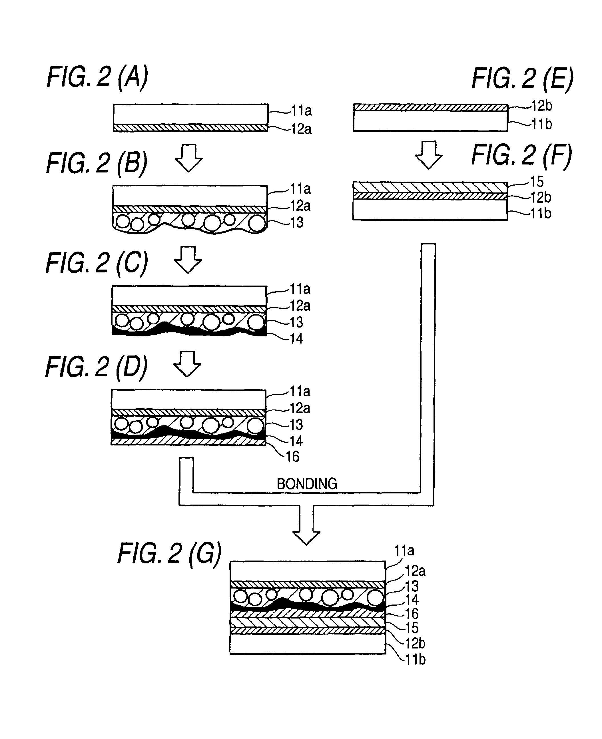
[0038]FIG. 2 is a proce...

second embodiment

[0097]FIG. 3 is a schematic process diagram, in cross section, showing a display element according to a second embodiment of the invention. In FIG. 3, the same or like parts are designated by the same numerals as in FIG. 1. In the second embodiment, the display element 1 of electric field writing type is shown. Namely, the photoconductive layer 15 is not provided.

[0098]On the substrate 11a, the electrode 12a, the display layer 13, the light shielding layer 14 and the adhesive layer 16 are laminated in the same manner as in the first embodiment, and as shown in FIG. 3(A). On the other hand, the electrode 12b is formed on the substrate 11b as shown in FIG. 3(B). The substrate 11a of FIG. 3(A) and the substrate 11b of FIG. 3(B) are bonded by the adhesive layer 16 to form the display element 1.

[0099]In the display element 1 of this construction, since the light shielding layer 14 is provided on the display layer 13, the excellent display quality can be obtained as with the first embodim...

third embodiment

[0103]FIG. 5 is a schematic process diagram, in cross section, showing a display element according to a third embodiment of the invention. In FIG. 5, the same or like parts are designated by the same numerals as in FIG. 1. In the first embodiment, the light shielding layer 14 as the display function layer is laminated on the display layer 13. However, the plurality of display function layers may be laminated on the display layer 13 and bonded with the substrate 11b. In this third embodiment, two display function layers are laminated on the display layer 13, and bonded with the substrate 11b.

[0104]The electrodes 12a and the display layer 13 are formed on the substrate 11a and the light shielding layer 14 and the photoconductive layer 15 are formed thereon, as shown in FIG. 5(A). The roughness on the surface of the display layer 13 are reduced by forming the light shielding layer 14, and further reduced by forming the photoconductive layer 15 to be almost flat in some cases.

[0105]The...


PUM

PropertyMeasurementUnit
visible wavelengthaaaaaaaaaa
volume average particle diameteraaaaaaaaaa
wavelengthaaaaaaaaaa

Abstract

A dispersion liquid including micro-capsules containing a cholesteric liquid crystal as a core material dispersed into a binder resin solution is applied to and dried on a substrate formed an electrode thereon to form a display layer. Then, a light shielding layer is formed and an adhesive layer is formed thereon. On the other hand, a photoconductive layer is formed on another substrate formed another electrode thereon. The substrate formed each layer thereon and the another substrate are bonded to form a display element. The light shielding layer 14 improves roughness on a surface of the display layer and the adhesive layer filled up the roughness. Even if the bubbles occur on a back face of the light shielding layer, the bubbles does not affect the display quality. Because the bubbles are unseen.

Description

[0001]The present disclosure relates to the subject matter contained in Japanese Patent Application No. 2002-276177 filed on Sep. 20, 2002, which is incorporated herein by reference in its entirety.BACKGROUND OF THE INVENTION[0002]1. Field of the Invention[0003]The present invention relates to a display element for displaying and recording an image, a document, and code information such as bar code and performing an optical information processing such as light modulation and optical switching using an optical change such as light transmission, light reflection, and light refraction, and a manufacturing method therefor.[0004]2. Description of the Related Art[0005]Conventionally, various display elements using a liquid display material such as a liquid crystal display element and an electrophoresis display element have been employed. To put such a display element into practical use, it is required to have a process of enclosing a display material into a “container” like a pair of subs...

Claims


Application Information

Patent Timeline
Patent Type & Authority Patents(United States)
IPC IPC(8): H01J9/00G02F1/1333G02F1/139G02F1/1334G02F1/1335G02F1/1339G02F1/135G09F9/00G09F9/35
CPCG02F1/133512G02F1/135G09F9/35G02F1/1334
Inventor HIJI, NAOKIYAMAMOTO, SHIGERU
Owner E INK CORPORATION
Why Eureka
Try Eureka