Method of wafer level packaging and cutting

a packaging and wafer technology, applied in the field of packaging and cutting, can solve the problems of mechanical force or particle contamination, destroy the structure of the package, and the conventional packaging method is quite complicated in batch production, so as to reduce the damage and contamination, reduce the yield loss, and simplify the cutting process

Inactive Publication Date: 2008-12-30
TOUCH MICRO SYST TECH
View PDF6 Cites 0 Cited by
  • Summary
  • Abstract
  • Description
  • Claims
  • Application Information

AI Technical Summary

Benefits of technology

[0006]It is therefore a primary objective of the claimed invention to provide a method of wafer level packaging and cutting to increase the yield and reliability of the packaging process.
[0008]The method of the invention may simplify the cutting process and diminish the damage and contamination resulting from the cutting process. The method may apply to electronic device packages, micro-electromechanical systems (MEMS) device packages, and optical device packages. In addition, the method of the invention reduces the yield loss caused by following processes, such as a cutting process, a breaking process, and a cleaning process. The method also has advantages of easy testing, high-yield, ease of batch production, and compatibility with general semiconductor processes.

Problems solved by technology

This damage may result from mechanical force or particle contamination.
In addition, the conventional packaging method is quite complicated in regards to batch production.
During cutting, mechanical force may destroy the structure of the package and particles may contaminate the product.
These conditions may reduce the yield of production.

Method used


Image

  • Method of wafer level packaging and cutting
  • Method of wafer level packaging and cutting
  • Method of wafer level packaging and cutting

Examples


Embodiment Construction

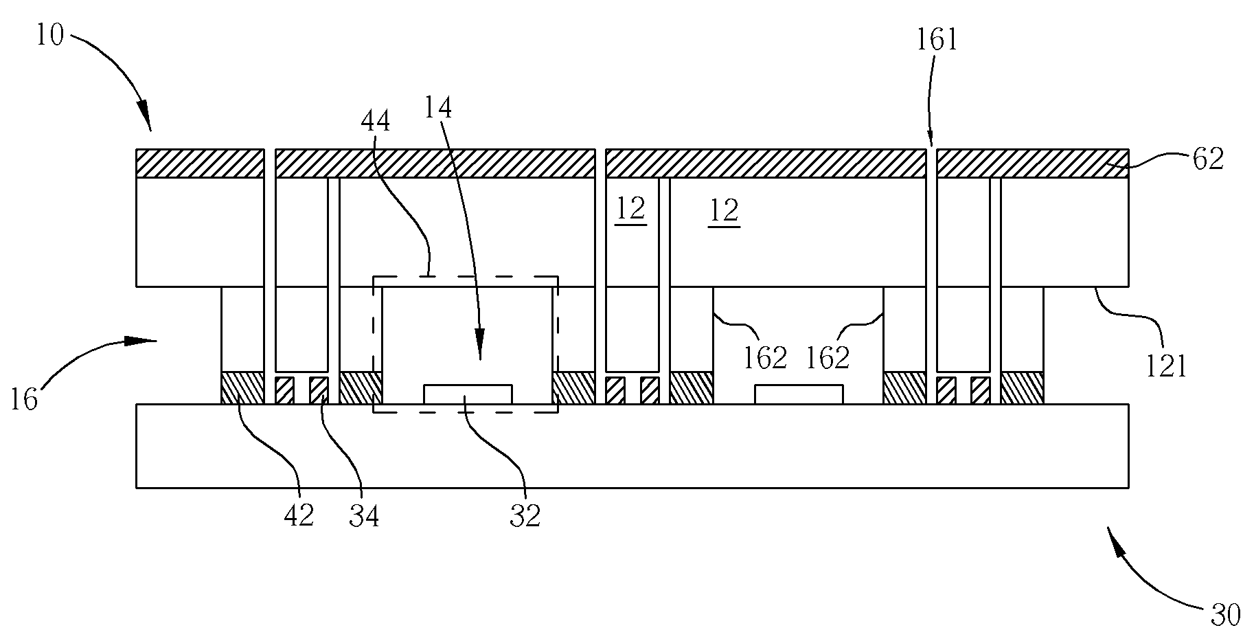
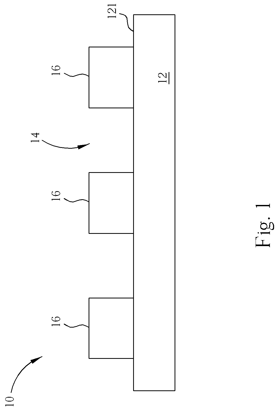
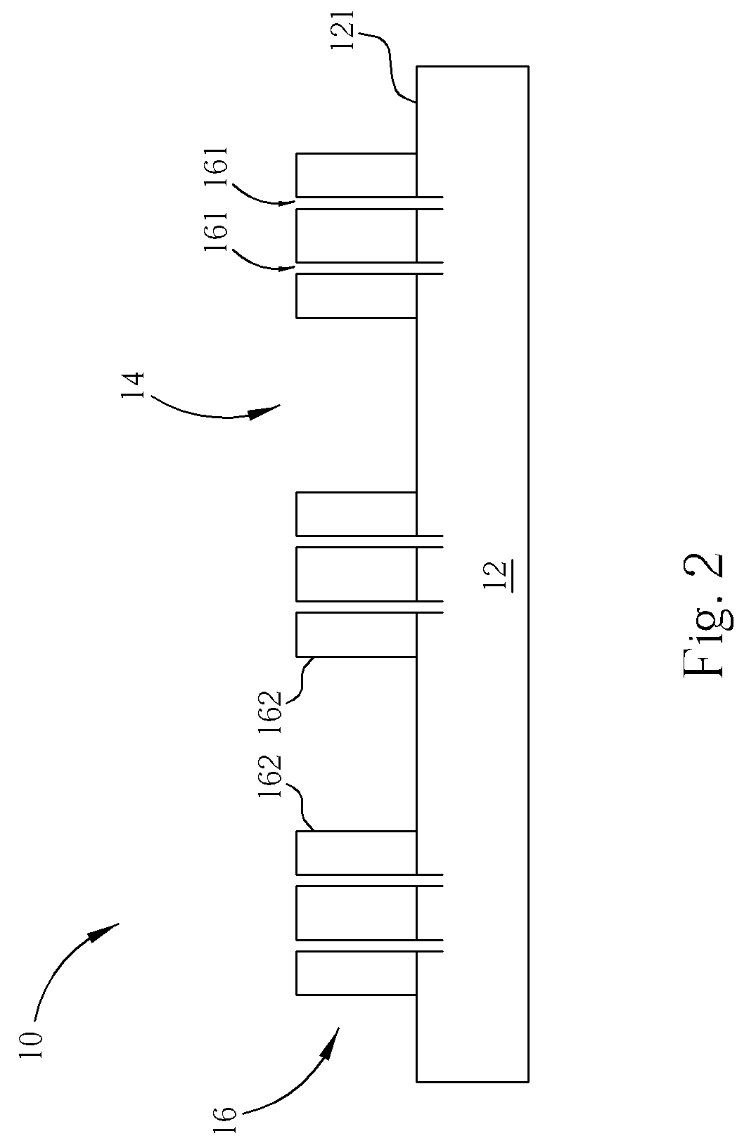
[0012]FIG. 1 through FIG. 9 are schematic diagrams illustrating a method of wafer level packaging and cutting according to a preferred embodiment of the invention. As shown in FIG. 1, a packaging wafer 10 is provided. The packaging wafer 10 comprises a transparent substrate 12, a pattern 16, and a plurality of cavities 14 defined by the pattern 16 on the front surface 121 of the transparent substrate 12. The transparent substrate 12 may comprise quartz, plastic, glass, or other light-transmissible materials. The transparent substrate 12 is a glass substrate in this embodiment. Please refer to FIG. 2. A pre-cutting process is performed upon predetermined positions of the packaging wafer 10. The pre-cutting process may be a wet wafer-cutting process, such as a wet etching process, or may be a dry wafer-cutting process, for instance, a dry etching process or cutting by blade. The pre-cutting process forms a plurality of trenches 161 on the pattern 16, and therefore defines a plurality ...


PUM


Abstract

A packaging wafer has a plurality of cavities and a plurality of trenches on a front surface thereof. The packaging wafer is bonded to the element wafer, and a first cutting method is performed. Afterward a piece of tape is provided and is attached to the packaging wafer. Moreover, a second cutting process is performed and then the piece of tape is removed. Therefore, a wafer level package is formed. In addition, the wafer level package is divided into a plurality of individual packages.

Description

BACKGROUND OF THE INVENTION[0001]1. Field of the Invention[0002]The invention relates to a method of packaging and cutting, and more particularly, to a method of wafer level packaging and cutting.[0003]2. Description of the Prior Art[0004]Packaging is an important step of semiconductor device fabrication. This process provides the core structure of the package to protect the fragile semiconductor device, such as optical device or micro-electromechanical systems (MEMS) device, from damage resulting from the environment. This damage may result from mechanical force or particle contamination. The package may also provide physical suspension and signal input / output.[0005]The conventional packaging method is illustrated as follows. A well-constructed wafer is divided to form a plurality of dies. Then, a die bonding process is performed such that each die is bound on a lead frame with epoxy. Furthermore, a wire-bonding process or a flip-chip process is performed to finish the packaging pr...

Claims


Application Information

Patent Timeline
Patent Type & Authority Patents(United States)
IPC IPC(8): H01L21/00
CPCB81C1/00269B81C2203/0118H01L21/78H01L27/14618H01L2924/0002H01L2924/00
Inventor WANG, SHUN-TA
Owner TOUCH MICRO SYST TECH
Why Eureka
Try Eureka