Stacked capacitor and method for producing stacked capacitors for dynamic memory cells

Inactive Publication Date: 2007-03-15
POLARIS INNOVATIONS
View PDF34 Cites 1 Cited by
  • Summary
  • Abstract
  • Description
  • Claims
  • Application Information

AI Technical Summary

Benefits of technology

[0018] In line with the invention, stacked capacitors are formed to have an insulating layer at their upper edge, so that it is not possible for a short circ

Problems solved by technology

If the capacitance of the storage capacitor is too small, the charge that is stored on the storage capacitor is too small to produce a reliably detectable signal.
In this case, the information stored in the memory cell is subject to large disturbances or is even lost and the memory cell does not work in the desired manner.
As structure sizes decrease, the wet etching and cleaning process steps described above become increasingly difficult, however.
However, it should be remembe

Method used


Image

  • Stacked capacitor and method for producing stacked capacitors for dynamic memory cells
  • Stacked capacitor and method for producing stacked capacitors for dynamic memory cells
  • Stacked capacitor and method for producing stacked capacitors for dynamic memory cells

Examples


first embodiment

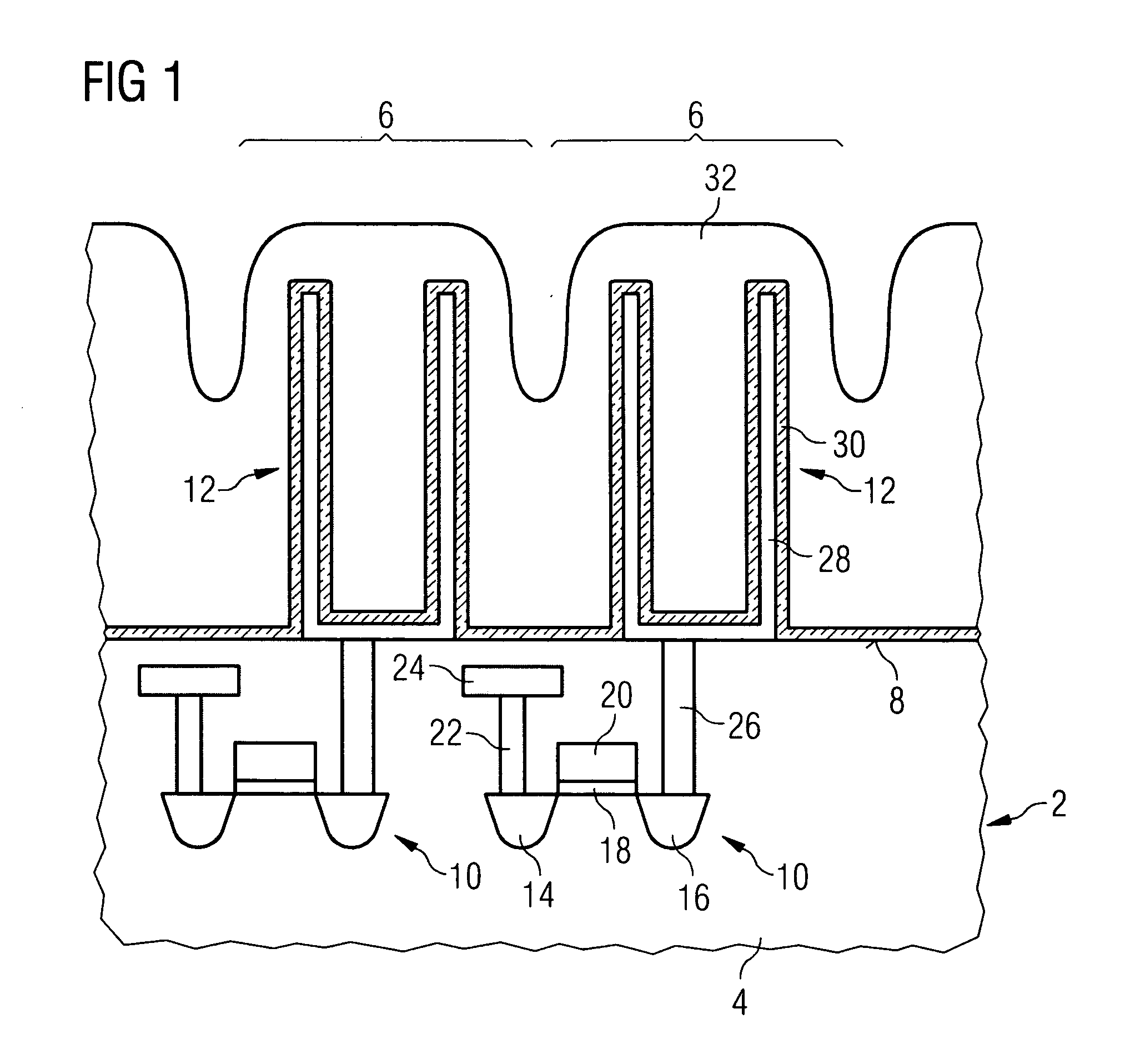
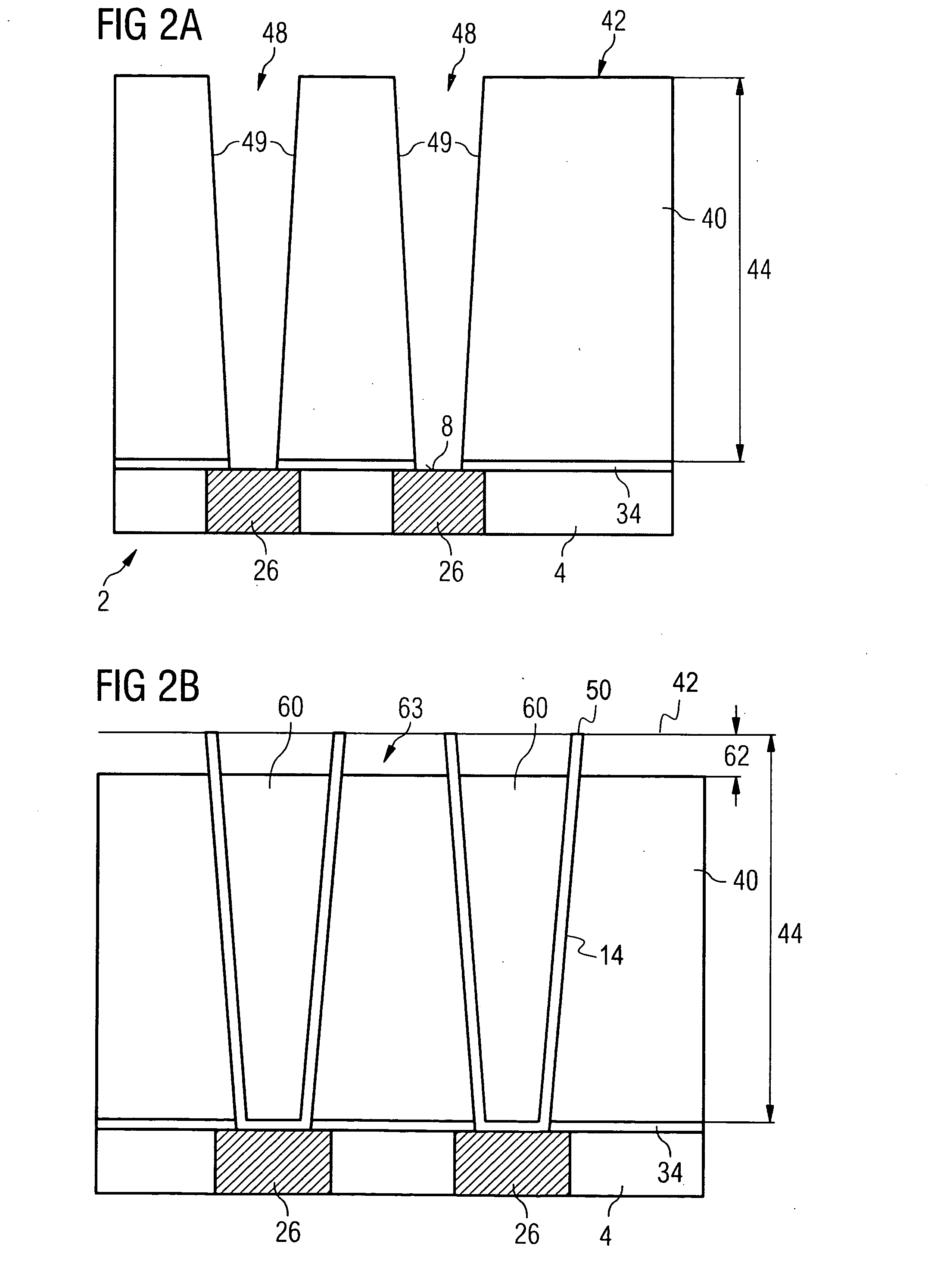
[0036] In a first process step, the method based on the invention provides the semiconductor wafer 2, which is used to produce the memory cells 6 with the stacked capacitors. The semiconductor wafer 2 comprises the substrate 4. In previous process steps, the transistors 10, bit lines 24 and other elements of the memory cell 6 are produced in the substrate 4. As FIG. 2A shows, the surface 8 of the substrate 4 has had an insulation layer 34 put on it, which leaves free the top of the contact plugs 26. The insulation layer 34 may comprise silicon nitride or silicon dioxide, for example. The contact plugs 26 preferably have a low resistance and are produced from amorphous silicon doped with arsenic, for example. In a production technology that has a minimum structure dimension of 70 nm, the contact plugs 26 are at a distance from one another, which is in the order of magnitude between 50 nm and 200 nm.

[0037] In another step, a masking layer 40 is deposited on the surface 8 of the substr...

second embodiment

[0052] In turn, the method based on the invention provides the semiconductor wafer 2 in a first process step, the semiconductor wafer being used to produce the memory cells 6 with the stacked capacitors 12. The semiconductor wafer 2 comprises the substrate 4.

[0053] As FIG. 3A shows, the surface 8 of the substrate 4 has had the insulation layer 34 put on it, leaving free some of the contact plugs 26. By way of example, the insulation layer 34 may comprise silicon nitride. The contact plugs 26 are made from polycrystalline silicon, for example.

[0054] In a further step, a masking layer 40 is deposited on the surface 8 of the substrate 4, on the insulation layer 34 and on the contact plugs 26. The masking layer 40 is provided by means of full-area deposition of a silicon dioxide layer, for example.

[0055] In the next step, a respective trench 48 is formed in the masking layer 40 for all memory cells 6. By way of example, the trenches 48 may be formed using a plasma etching process. To ...

third embodiment

[0074] In a first process step, the method based on the invention again provides the semiconductor wafer 2, which is used to produce the memory cells 6 with the stacked capacitors 12 (FIG. 1). The semiconductor wafer 2 comprises the substrate 4. In a further step, a masking layer 40 is deposited on the surface 8 of the substrate 4 and on the contact plugs 26.

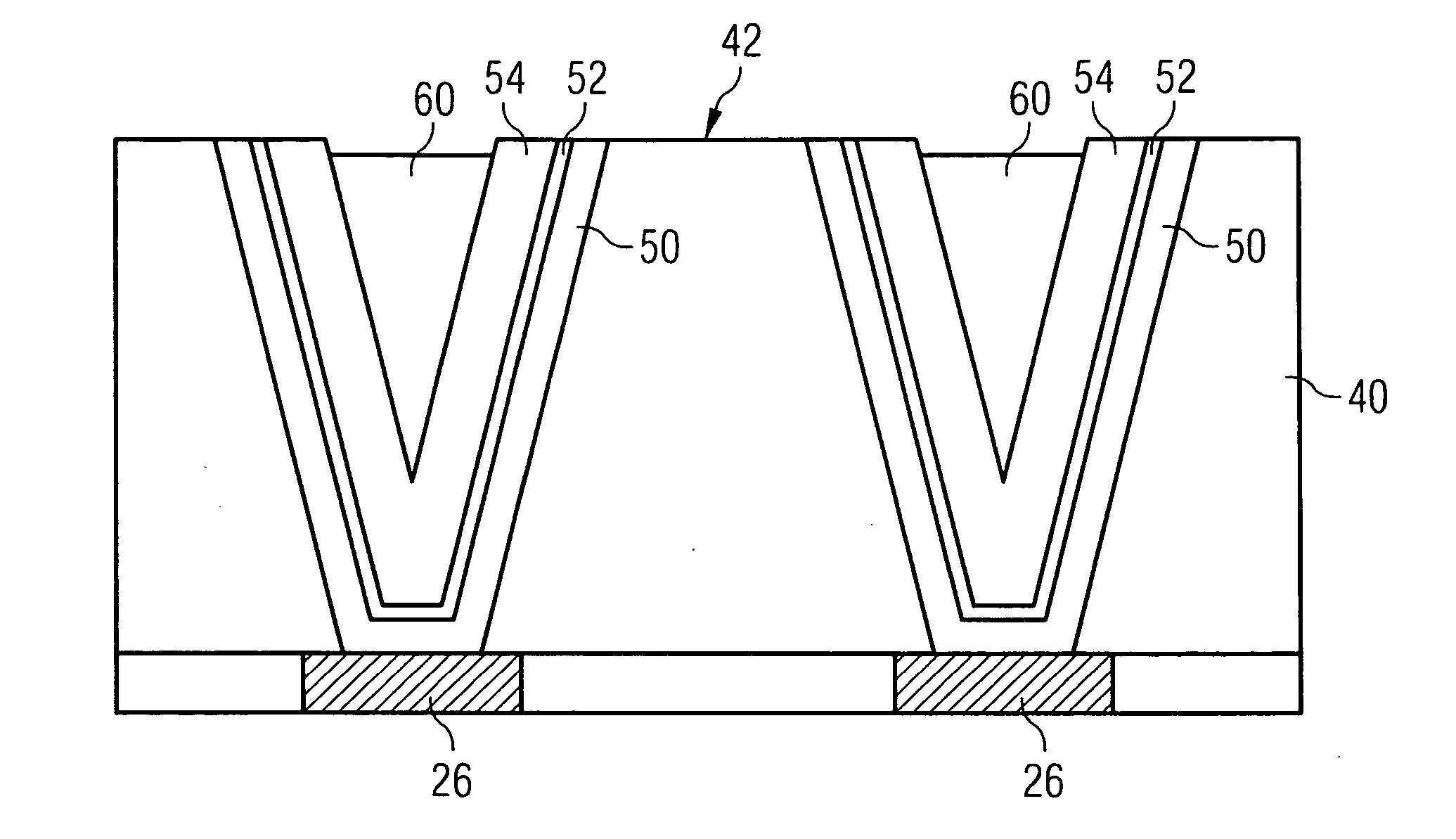
[0075] In the next step, a respective trench 48 is formed in the masking layer 40 for all memory cells 6. Each of the trenches 48 is arranged above the associated contact plug 26 and extends from the top 42 of the masking layer 40 to the contact plugs 26 on the top 8 of the semiconductor wafer 2. Each of the trenches 48 has side walls 49 that may be perpendicular or slightly inclined, for example, as FIG. 5A shows.

[0076] As FIG. 5B shows, the conductive layer 50 is formed over the semiconductor wafer 2 in a subsequent process step.

[0077] In a subsequent process step, a dielectric layer 52 is formed over the semiconductor wafer...


PUM


Abstract

A method produces stacked capacitors for dynamic memory cells, in which a number of trenches (48) are formed in the masking layer (40), each trench (48) being arranged above a respective contact plug (26) and extending from the top (42) of the masking layer (40) to the contact plugs (26). A conductive layer (50) covers the side walls (49) of the trenches (48) and the contact plugs (26) in order to form a first electrode (60) of a stacked capacitor (12). In an upper region (63), which is remote from the contact stack (26), the conductive layer (50) is replaced by an insulating layer, so that it is not possible for a short circuit to arise in the event of any adhesion between adjacent electrodes.

Description

[0001] This application claims priority to German Patent Application 10 2005 042 524.0 which was filed Sep. 7, 2005 and is incorporated herein by reference. TECHNICAL FIELD [0002] The invention relates to a stacked capacitor for dynamic memory cells. The invention also relates to methods for producing stacked capacitors for dynamic memory cells. BACKGROUND [0003] When producing integrated circuits, attempts are made at continuously reducing the structure sizes of the components produced. For particular circuit elements, such as capacitors, reducing the structure dimensions influences the electrical properties. To guarantee a minimum value for the capacitance of a storage capacitor which should be exceeded, for example, a particular surface area of the capacitor must therefore be above a prescribed value. This is particularly important for dynamic random access memories (DRAMs), for which a large scale of integration is pursued. [0004] When the surface area on a semiconductor wafer's...

Claims


Application Information

Patent Timeline
IPC IPC(8): H01L21/336
CPCH01L27/10814H01L28/90H01L27/10852H10B12/315H10B12/033
Inventor KUDELKA, STEPHANMOLL, PETERJAKSCHIK, STEFANWUNNICKE, ODO
Owner POLARIS INNOVATIONS
Why Eureka
Try Eureka