Sensor for intravascular measurements within a living body

a technology of intravascular measurement and living body, which is applied in the field of pressure sensors to achieve the effect of improving the sensitivity of the sensor

Active Publication Date: 2009-01-06
ST JUDE MEDICAL COORDINATION CENT
View PDF12 Cites 43 Cited by
  • Summary
  • Abstract
  • Description
  • Claims
  • Application Information

AI Technical Summary

Benefits of technology

[0006]In one embodiment of the present invention, a Wheatstone bridge-type of arrangement is disclosed, wherein, however, a conventional piezoresistive element has been replaced by a so-called nanowire. A nanowire is a wire having dimensions of the order of one nanometer (10−9 meters), and can be defined as a structure that has a lateral size constrained to tens of manometers or less and an unconstrained longitudinal size. A nanowire can be made from carbon (C) or a metal, such as nickel (Ni), platinum (Pt), or gold (Au); or a semiconductor, such as silicon (Si), indium phosphide (InP), or gallium nitride (GaN); or insulators like silicon dioxide (SiO2) and titanium dioxide (TiO2). Several of these nanowires exhibit a pronounced piezoresistive behaviour, which in the field also is referred to as the giant piezoresistance effect. The piezoresistive behaviour is usually due to a change in conductance when the nanowire is subjected to stress caused by stretching and / or compression. According to the invention, a guide wire mounted sensor comprises a sensor element, which, in turn, comprises at least one nanowire exhibiting a piezoresistive effect, which is exploited in order to improve the sensitivity of the sensor. As defined herein, it should further be noted that the term “piezoresistive nanowire” also encompasses nanowires made from materials that do not exhibit a piezoresistance effect in themselves; examples of such materials are zinc oxide (ZnO) and aluminium nitride (AlN). In nanowires made from these materials, the piezoresistive behaviour is believed to be caused by a charge rearrangement, which takes place when the nanowire is subjected to stress. Generally, the term “piezoresistive nanowire” as used herein encompasses all kinds of nanowires and wire-like structures such as nanowhiskers, nanorods, nanotubes, nanocantilevers, etc. whose electrical resistance changes when they are deformed (e.g. compressed or stretched) due to the influence of pressure. It should also be noted that a nanowire according to the invention can have any cross-sectional shape. In a preferred embodiment, the cross-section is solid and circular, but it is also contemplated that a nanowire can have a ring-shaped cross-section, i.e. the nanowire is in fact a nanotube. In another embodiment, the cross-section could be quadratic or rectangular. In the latter case, the nanowire could have the shape of a thin and flat strip. The latter embodiment could be advantageous not least from a production point of view.

Problems solved by technology

As will be more clearly explained below, due to the rather low sensitivity of the sensor, such a high resistivity puts corresponding requirements on the insulation of the sensor element and also on other parts of the sensor and guide wire assembly.

Method used


Image

  • Sensor for intravascular measurements within a living body
  • Sensor for intravascular measurements within a living body
  • Sensor for intravascular measurements within a living body

Examples


first embodiment

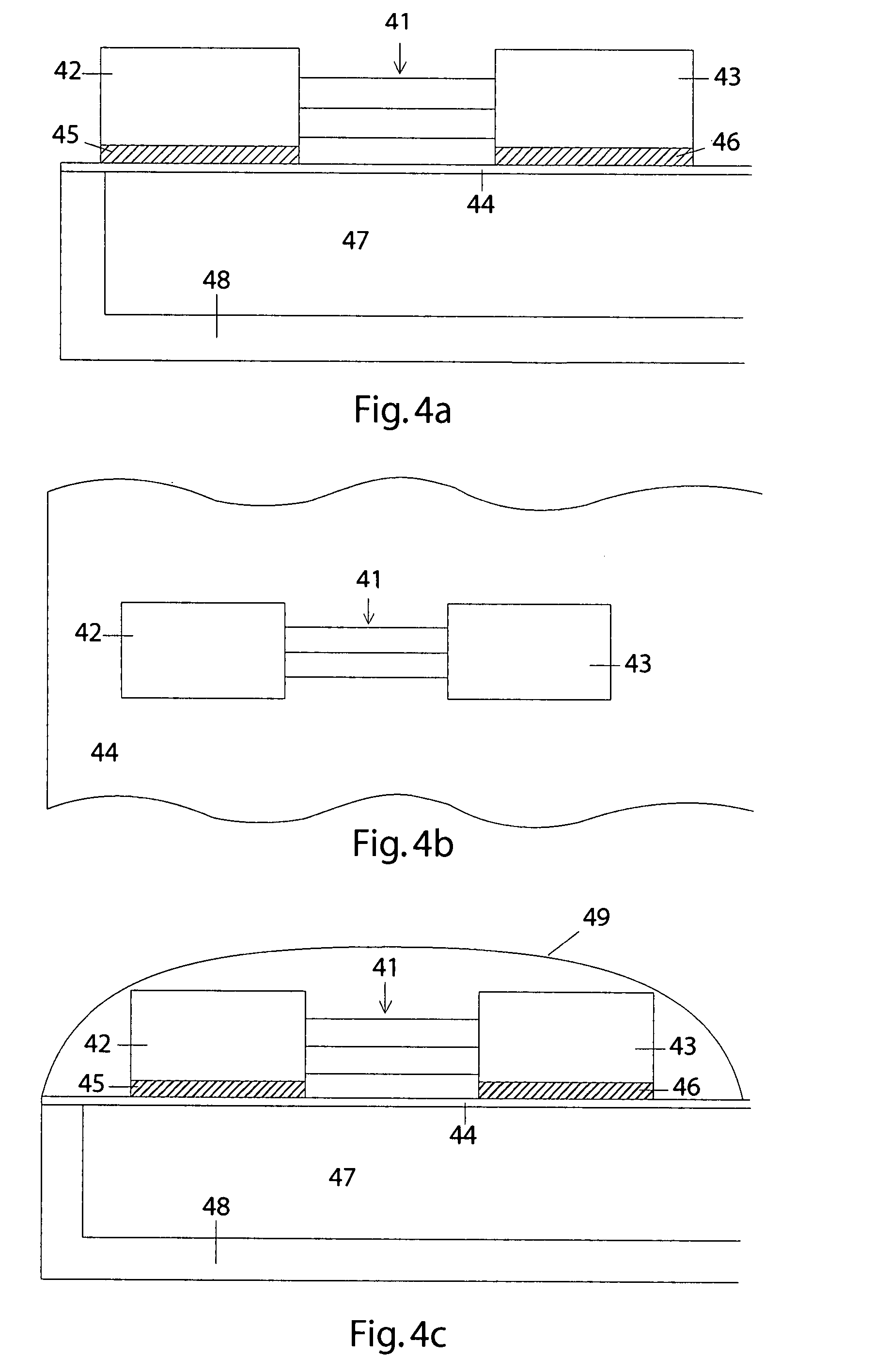
[0022]The present invention is directed to a sensor and guide wire assembly comprising a piezoresistive element in the form of a nanowire. In the invention, at least one nanowire is arranged on a membrane in a way similar to the arrangements shown in conjunction with FIG. 2 and FIG. 3, respectively. More specifically, FIG. 4a (which is a side view) and b (which is a top view) illustrate schematically how several piezoresistive nanowires 41 (in this case nine nanowires) extend between a first terminal 42 and a second terminal 43, which are attached to the upper side of a flexible membrane 44, from which the terminals 42 and 43 are electrically insulated by insulating layers 45 and 46, respectively. The membrane 44 covers an evacuated cavity 47 made in a chip 48 made from, for example, silicon; and when the membrane 44 deflects due to influence from the ambient pressure (e.g. blood pressure), the nanowires 41 will be stretched, and their (total) electrical resistance will thereby chan...

second embodiment

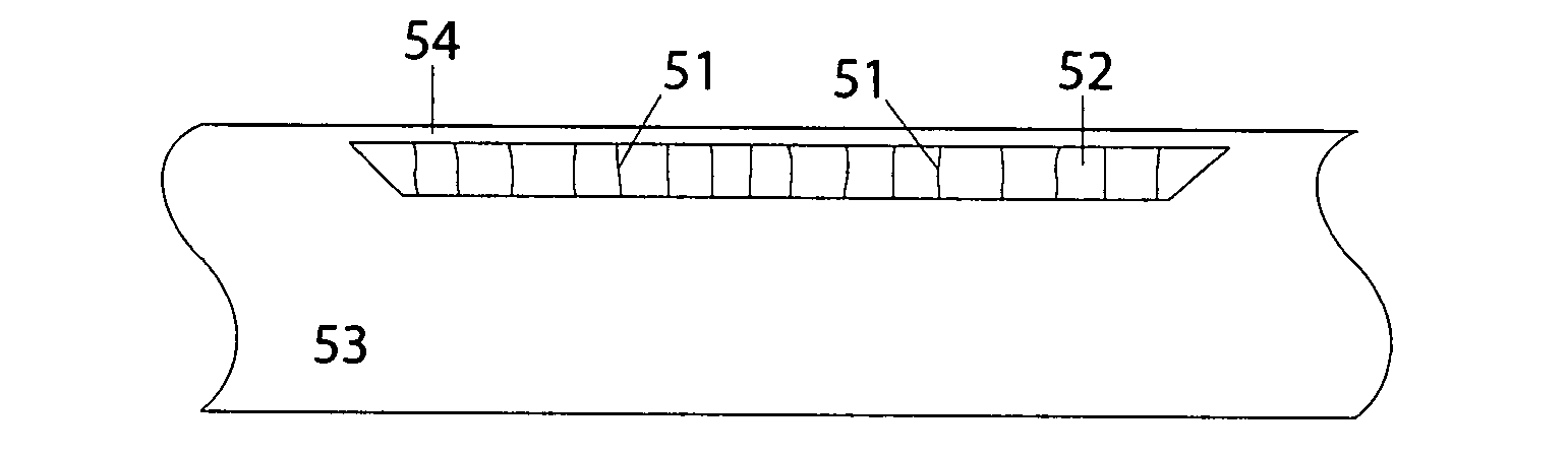
[0024]In FIGS. 5a and 5b the present invention is disclosed. Here, a number of piezoresistive nanowires 51 (in this case sixteen nanowires) have been arranged within a cavity 52 created by a recess in a chip 53, which recess is covered by a membrane 54. More specifically, the nanowires 51 extend between the bottom surface of the cavity 52 and the membrane 54, such that when the membrane 54 deflects downwards due to influence of the ambient pressure (typically blood pressure), the nanowires 51 are compressed (see FIG. 5b), which leads to a corresponding change in their total resistance. The resistance change can be exploited to determine the applied pressure.

third embodiment

[0025]FIG. 6 shows the present invention, wherein a large number of piezoresistive nanowires 61 are arranged within a double-walled membrane 62, which comprises an inner wall 63 and an outer wall 64. The membrane 62 covers a recess which has been made in a chip 65. Like before, deflection of the membrane 62 will cause the nanowires 61 to compress, which, in turn, leads to a resistance change that can be detected by a suitable electrical circuit.

[0026]As was explicitly discussed in conjunction with FIG. 4c, it can be advantageous to provide the nanowires with some insulation against ambient fluid. The insulation problem can be solved by arranging the nanowires beneath a flexible membrane; and in FIG. 7 an exemplifying embodiment of such an arrangement is disclosed. In this embodiment, several nanowires 71 extend between a first terminal 72 and a second terminal 73, which are attached to the underside of a flexible membrane 74, from which the terminals 72 and 73 are electrically insul...


PUM


Abstract

The invention relates to a sensor and guide wire assembly for intravascular measurements within a living body, wherein a sensor element, which is arranged at a distal portion of a guide wire, comprises at least one piezoresistive nanowire.

Description

FIELD OF THE INVENTION[0001]The invention relates generally to a pressure sensor mounted on a guide wire for intravascular measurements of pressure in a living body, and in particular to the design of a piezoresistive element, which is part of the pressure sensor and whose piezoresistive effect is utilized for pressure measurements.BACKGROUND OF THE INVENTION[0002]Sensor and guide wire assemblies in which a sensor, adapted for measurements of physiological variables in a living body, such as blood pressure and temperature, is mounted at a distal portion of a guide wire are known.[0003]For example, the U.S. Pat. No. Re. 35,648, which is assigned to the present assignee and incorporated herein by reference for the devices and techniques disclosed therein, discloses a sensor and guide wire assembly comprising a sensor element, an electronic unit, signal transmitting cables connecting the sensor element to the electronic unit, a flexible tube having the signal cables and the sensor elem...

Claims


Application Information

Patent Timeline
Patent Type & Authority Patents(United States)
IPC IPC(8): A61B5/00
CPCA61B5/0215A61B5/6851A61M25/09A61B2562/02A61B2562/0247A61B2562/0285
Inventor TENERZ, LARSSMITH, LEIF
Owner ST JUDE MEDICAL COORDINATION CENT
Why Eureka
Try Eureka