Latch circuit

a latch circuit and circuit technology, applied in the field of latch circuits, can solve the problems of permanent damage to a specific portion of the circuit, soft error, circuit malfunction, etc., and achieve the effect of increasing the soft error resistance, minimizing the increase in the area occupied, and not decreasing the response speed of the circui

Active Publication Date: 2009-01-06
SOCIONEXT INC
View PDF3 Cites 7 Cited by
  • Summary
  • Abstract
  • Description
  • Claims
  • Application Information

AI Technical Summary

Benefits of technology

[0011]Accordingly, an object of the present invention is to provide a latch circuit that minimizes an increase in the area occupied by logic circuits and that increases the soft error resistance so as to prevent a decrease in the circuit response speed.
[0016]Accordingly, even when a soft error occurs in one of the input terminals and an input signal in a malfunction state is input, no feedback is applied to the input terminal or positive feedback using a larger number of amplification stages than a predetermined number of amplification stages is applied. With this arrangement, the possibility that a malfunction state due to a soft error becomes stationary is reduced.
[0017]On the other hand, during a normal operation in which input signals are input to the at least two input terminals at the same time, positive feedback using a predetermined number of stages is applied. Thus, the response speed of the circuits does not decrease.
[0018]Accordingly, the present invention can provide a latch circuit that minimizes an increase in the area occupied by logic circuits and that increases the soft error resistance so as to prevent a decrease in the circuit response speed.

Problems solved by technology

It has been known that a rays generated upon collapsing of radioactive isotopes contained in packages or wires in LSI (large scale integration) semiconductor circuits, neutron radiation derived from cosmic rays, and so on produce electrical noise in the LSI semiconductor circuits to thereby cause the semiconductor circuits to malfunction.
Such malfunction is called soft error as opposed to hard error caused by failures in hardware, such as semiconductor circuits.
Thus, the soft error is different from the hard error in that the soft error causes a transient malfunction in which the operation can be resumed but the hard error causes a permanent damage to a specific portion of a circuit.
However, when a transient malfunction due to soft error is stored in a latch circuit included in an SLI semiconductor circuit, the malfunction due to the soft error can become a stationary error in the semiconductor circuit.
In this case, with advancements in high-integration and microfabrication technologies and reductions in charge capacities of storage nodes in latch circuits included in LSI semiconductor circuits, the probability that a soft error resulting from the generation of electrical noise becomes a stationary error increases.
This is because electrical noise facilitates the inversion of the logic states of the storage nodes of the latch circuits and thus the frequency of occurrence of malfunction states increases.
However, in the error preventing method, for example, since the circuitry is configured so as to obtain parity, the number of circuits and the area of the circuitry increase, which causes a reduction in the circuitry performance.
The arrangement, however, does not increase the soft error resistance of the dynamic latches included in the feedback loops.
Thus, there is a problem in that a malfunction state due to soft error in the dynamic latches becomes stationary.
Accordingly, there is a problem in that, when malfunction states due to soft errors in two dynamic latches become stationary at the same time, the malfunction due to the soft errors becomes a stationary error in the semiconductor circuit.
Thus, there is a problem in that the area occupied by logic circuits increases or the response speed of the circuits decreases.

Method used


Image

  • Latch circuit
  • Latch circuit
  • Latch circuit

Examples


first embodiment

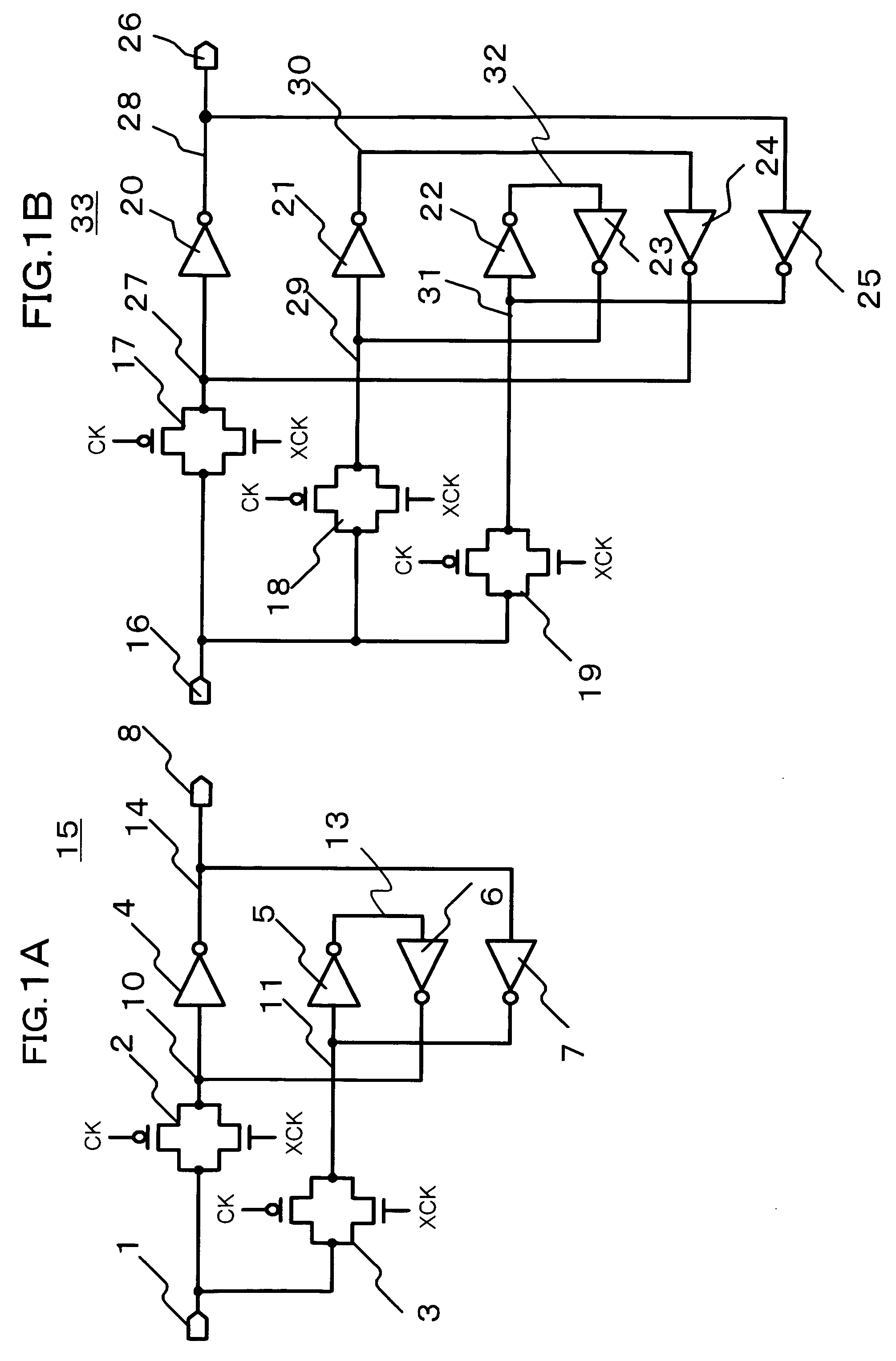
[0029]A first embodiment is directed to a latch circuit that features the use of multiple inverter circuits at four or more even number of stages to feed back signals. The first embodiment is also directed to a latch circuit having a configuration in which input signals are transmitted to multiple nodes and are fed back by two-stage inverter circuits. In the latching according to the first embodiment, since the time required for the feedback is increased, there is an advantage in that the time taken until a malfunction state occurred due to soft error becomes stationary increases. On the other hand, since the input signals are transmitted to the multiple nodes, there is an advantage in that the response speed of the latch circuit is maintained. The first embodiment will now be described with reference to FIGS. 1A, 1B, 2, 3A, and 3B.

[0030]FIGS. 1A and 1B each show a latch circuit that includes inverter circuits at four or more even number of stages and that have multiple nodes to whi...

second embodiment

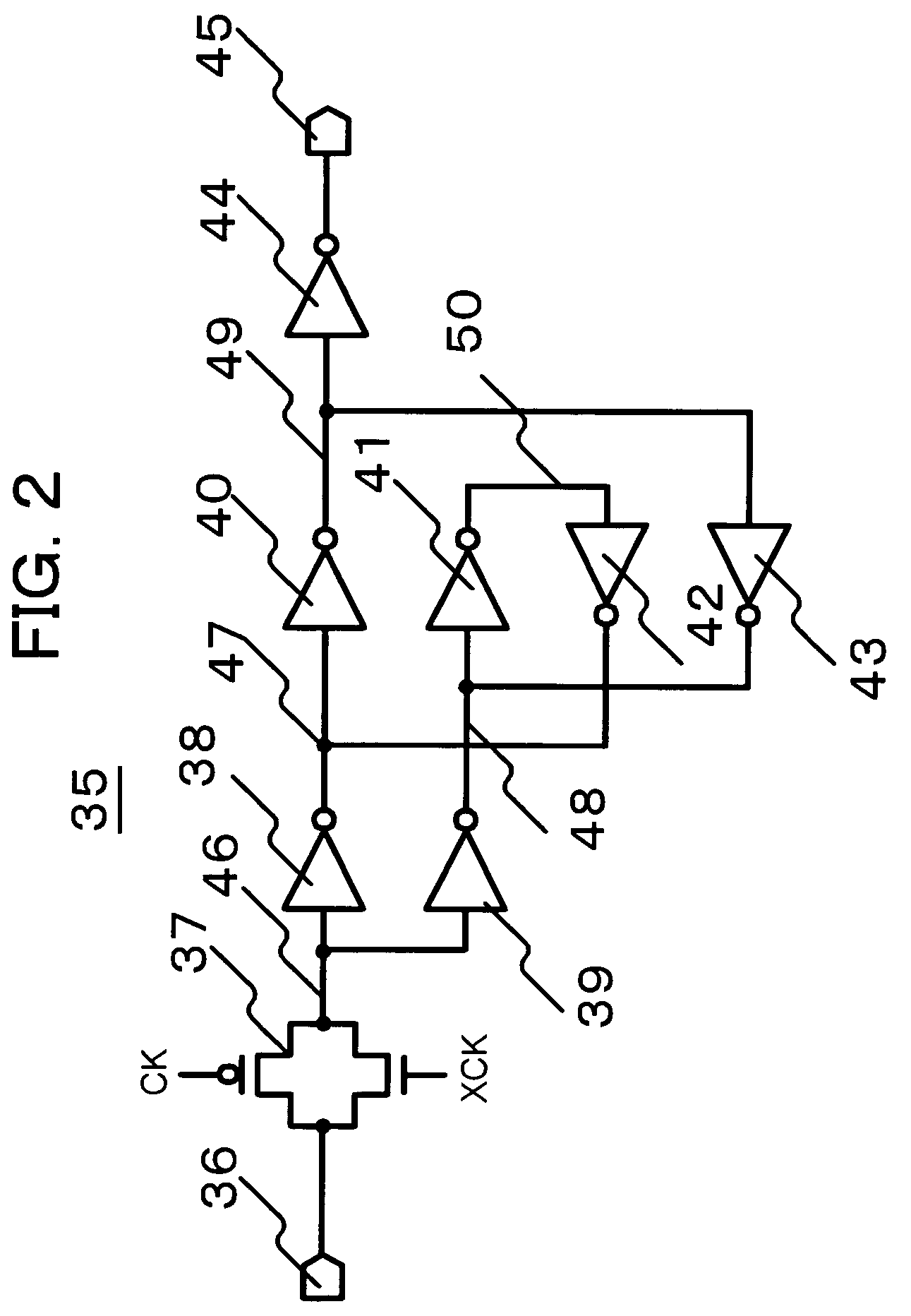
[0056]A second embodiment is directed to a latch circuit having a configuration in which a feedback circuit includes an inverter circuit having two input terminals and one output terminal so as to prevent feedback from being applied to a connection node having a logic level in a malfunction state. The second embodiment is also directed to a latch circuit having a configuration in which input signals input to two input terminals are fed back using feedback paths provided by two-stage inverter circuits. In the latching according to the second embodiment, since no feedback is applied to a connection node in a malfunction state, there is an advantage in that an error caused by soft error does not become stationary. In addition, since multiple feedback paths to which input signals are input are each constituted by two-stage inverter circuits, there is an advantage in that the response speed of the latch circuit is maintained. The second embodiment will now be described with reference to ...

third embodiment

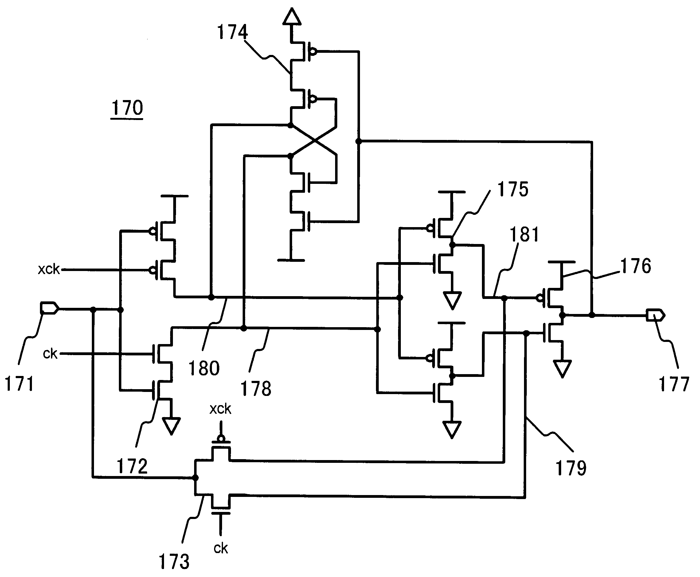
[0106]A third embodiment is directed to a latch circuit having a configuration in which a feedback circuit includes an inverter circuit having two input terminals and two output terminals so as to prevent feedback from being applied to a connection node having a logic level in a malfunction state. The third embodiment is also directed to a latch circuit having a configuration in which input signals input to two input terminals are fed back involving two-stage amplification. In the latching according to the third embodiment, since no feedback is applied to a connection node in a malfunction state, there is an advantage in that an error generated by soft error does not become stationary. In addition, since feedbacks to the input terminals of the inverter circuits are implemented with predetermined two-stage inverter circuits, there is an advantage in that the response speed of the latch circuit is maintained. Now, the third embodiment will be described with reference to FIG. 8.

[0107]F...


PUM


Abstract

A latch circuit includes a feedback circuit having inverter circuits and at least two input terminals and an input circuit for inputting input signals or signals having the same phase as the input signals to the input terminals of the feedback circuit in synchronization with a clock signal. In the feedback circuit section, only when the input signals or the signals having the same phase as the input signals are input to the at least two input terminals at the same time, positive feedback using a predetermined number of amplification stages is applied to the input terminals.

Description

BACKGROUND OF THE INVENTION[0001]1. Field of the Invention[0002]The present invention relates to semiconductor circuits including logic circuits. In particular, the present invention relates to a semiconductor circuit including a latch circuit in which occurrence of soft error is suppressed.[0003]2. Description of the Related Art[0004]It has been known that a rays generated upon collapsing of radioactive isotopes contained in packages or wires in LSI (large scale integration) semiconductor circuits, neutron radiation derived from cosmic rays, and so on produce electrical noise in the LSI semiconductor circuits to thereby cause the semiconductor circuits to malfunction. Such malfunction is called soft error as opposed to hard error caused by failures in hardware, such as semiconductor circuits. Thus, the soft error is different from the hard error in that the soft error causes a transient malfunction in which the operation can be resumed but the hard error causes a permanent damage t...

Claims


Application Information

Patent Timeline
Patent Type & Authority Patents(United States)
IPC IPC(8): H03K19/003
CPCH03K3/356156H03K19/003H03K19/00315H03K19/0033
Inventor UEMURA, TAIKITOSAKA, YOSHIHARU
Owner SOCIONEXT INC
Why Eureka
Try Eureka