Clock and data recovery method and digital circuit for the same

Inactive Publication Date: 2009-01-06
HITACHI LTD
View PDF19 Cites 17 Cited by
  • Summary
  • Abstract
  • Description
  • Claims
  • Application Information

AI Technical Summary

Benefits of technology

[0050]From another point of view of the present invention, the present invention is characterized by including a control circuit for executing control so as to place the edge of a data recovery clock signal in an eye narrowed by jitters, which are high-frequency components of data, by comparing the position of the edge of the data recovery clock signal with the position of the edge of the data, wherein the data is then taken in with a timing of the edge of the data recovery clock signal. Thus, the control circuit executes control so that the distance between the position of the edge of the data recovery clock signal and the position of the edge of the data does not become smaller than a predetermined value. That is to say, the control circuit is capable of executing control so as to place the edge of the data recovery clock signal in an eye narrowed by jitters,

Problems solved by technology

Thus, the CDR circuit is not suitable for bit-count enhancement of an optical transmission system.
In addition, data may not be taken in correctly in dependence on the quantity Tb of the wander.
(1) The configuration of the conventional clock data recovery circuit does not include sufficient consideration of an edge detection method for data with a jitter width exceeding 0.5 UI. That is to say, let data with a jitter width exceeding 0.5 UI be handled by adoption of an edge detection technique based on an edge-tracking method. In this case, if the phase of a data edge on the eye side is compared with the phase of a clock rising edge, an edge for recovery of data on the clock falling edge is shifted out from the data recovery width. As a result, the data cannot be recovered correctly. In other words, the edge-tracking method can correctly recovery only data with a jitter width of about 0.5 UI or below.
As is obvious from the above description, the clock data recovery circuit described above has a problem of a poor jitter-tolerance characteristic.
(2) The configuration

Method used


Image

  • Clock and data recovery method and digital circuit for the same
  • Clock and data recovery method and digital circuit for the same
  • Clock and data recovery method and digital circuit for the same

Examples


first embodiment

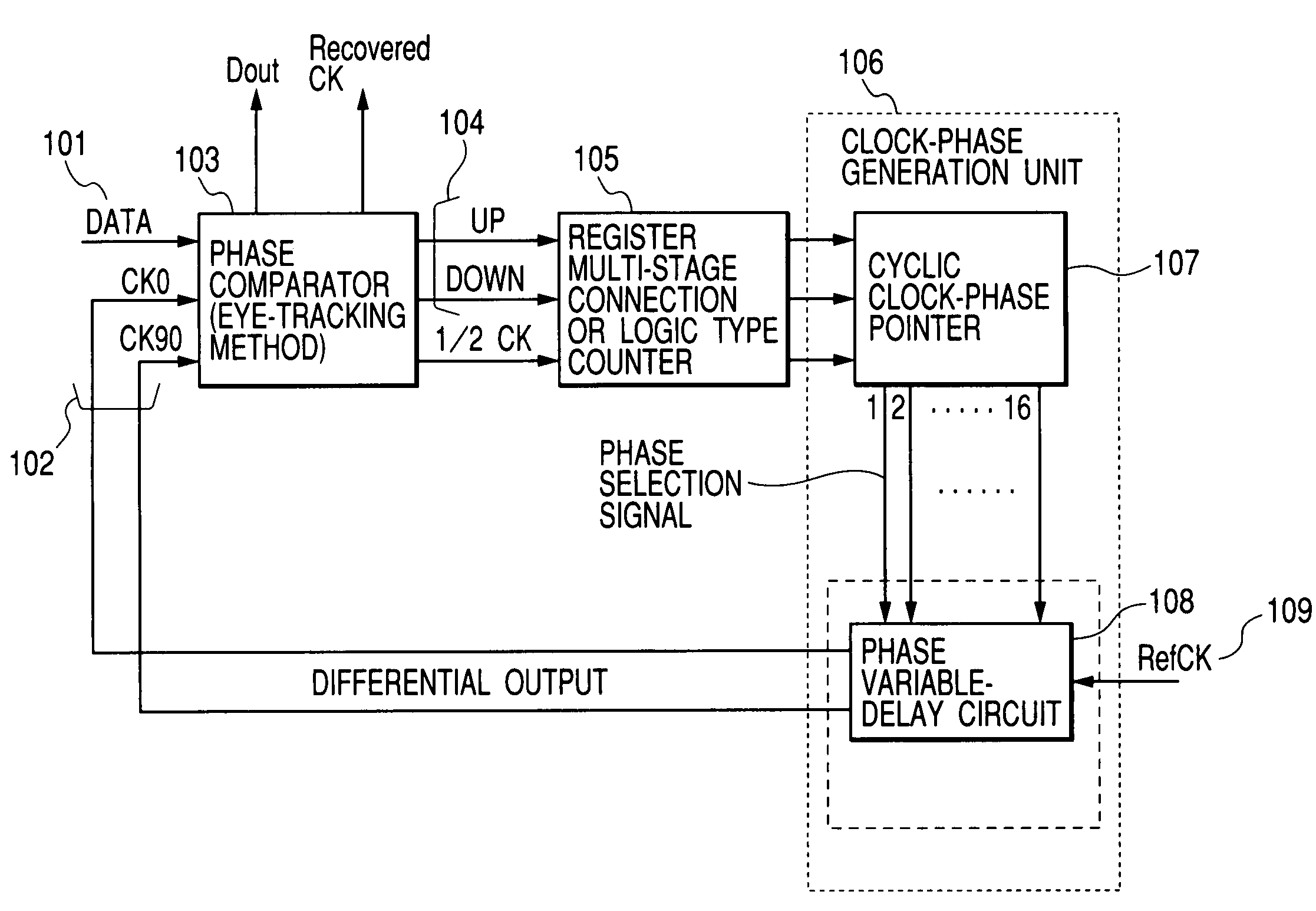
[0081]FIG. 1 is a block diagram showing the configuration of a digital-control type clock data recovery circuit implemented by the present invention. The digital-control type clock data recovery circuit is also referred to hereafter simply as a digital clock data recovery circuit.

[0082]As shown in FIG. 1, the digital clock data recovery circuit comprises: a phase comparator 103 for comparing the phase of input data 101 with the phase of a data recovery clock signal 102 generated internally and outputting shift directions of the phase of the data recovery clock signal 102 as UP and DOWN signals 104; a register multi-stage connection OR logic type counter 105 for controlling a frequency at which the UP and DOWN signals 104 are fed back to a means for determining the phase of the data recovery clock signal 102; and a clock-phase generation unit 106 for generating an output phase of the data recovery clock signal on the basis of signals output by the counter 105.

[0083]The clock-phase ge...

second embodiment

[0123]FIG. 12 is a circuit diagram showing a phase variable-delay circuit 1200 implemented by the present invention. As shown in FIG. 12, the phase variable-delay circuit 1200 typically comprises buffers 1201, composition circuits 1202, 8-1 selectors 1203 shown in FIG. 13 and CMOS level conversion circuits 1204. The buffers 1201 are each a memory for storing 0-degree / 90-degree clock inputs. The composition circuits 1202 form a unit for generating 8 signals having phases different from each other from 2 signals having phases different from each other. The 8-1 selectors 1203 form a unit for treating the 8 signals with phases different from each other as 16 signals having 16 different selectable phases and selecting a phase from the 16 phases. In order to output a 0-degree differential clock signal and a 90-degree differential clock signal, the 8-1 selectors 1203 and the CMOS level conversion circuits 1204 are each designed as a dual component. The 0-degree differential clock signal an...

third embodiment

[0130]FIG. 14 is a block diagram showing the configuration of a digital clock data recovery circuit implemented by the present invention.

[0131]As shown in FIG. 14, the digital clock data recovery circuit comprises: a phase comparator 1403 for comparing the phase of input data 1401 with the phase of a data recovery clock signal 1402 generated internally and outputting a shift direction of the phase of the data recovery clock signal 1402 as UP and DOWN signals 1404; a register multi-stage connection OR logic type counter 1405 for controlling a frequency at which the UP and DOWN signals 1404 are fed back to a means for determining the phase of the data recovery clock signal 1402; and a clock-phase generation unit 1406 for generating an output phase of the data recovery clock signal on the basis of signals output by the counter 1405.

[0132]The clock-phase generation unit 1406 comprises a cyclic clock-phase pointer 1407 and a digital-control type phase variable-delay circuit 1408.

[0133]Si...


PUM


Abstract

A clock data recovery circuit has a good jitter tolerance characteristic and a broad data recovery range in the event of a wander, that is, a good wander-tracking characteristic of a recovered clock signal. The clock data recovery circuit executes control to compare the position of the edge of data with the position of the edge of a data recovery clock signal (a recovered clock signal) and keeps the clock edge away from the data edge if a gap between the edges becomes smaller than a reference value. A cycle of a reference clock signal is divided into N portions to generate N clock signals (pl ) with phases different from each other in composition circuits. By executing control to turn on 2 of the N selector control signals supplied to each 2 adjacent pins of the N−1 selectors at the same time, the N−1 selectors are capable of generating a middle phase between first and second phases and, hence, generating one of N×2 phases from N input phases as the phase of the data recovery clock signal.

Description

FIELD OF THE INVENTION[0001]The present invention relates to a digital clock / data recovery circuit that has a good jitter / wander-tolerance characteristic as well as allows its size and its power consumption to be reduced with ease.BACKGROUND OF THE INVENTION[0002]With a remarkably increasing number of data communication services due to, among others, the popularization of the Internet in recent years, an optical transmission system using optical fibers is applied to mainly trunk networks in a wide range of networks up to metro networks. Nowadays, it is time to implement production of a 10-Gbps optical transmission system for trunk networks on a full scale. In addition, development of a communication LSI for a next-generation optical transmission system with a transmission speed of 40 Gps has been started. So far, in an interface of a Framer IC for an optical transmission module, there has been adopted a transmission system for transmitting data and a clock signal in parallel.[0003]N...

Claims


Application Information

Patent Timeline
IPC IPC(8): H04L7/00H04J3/06H03L7/081H03L7/091H04L7/02H04L7/033
CPCH03L7/0814H03L7/091H04L7/0331H04L7/0337H03L2207/50
Inventor YUUKI, FUMIOYAMASHITA, HIROKISONEHARA, MASAHITO
Owner HITACHI LTD
Why Eureka
Try Eureka