Plasma process apparatus and its processor
a processing apparatus and processing technology, applied in the field ofplasma processing apparatus and processing apparatus, can solve the problems of difficult effective optimization difficult effective improvement of microwave propagation efficiency within the dielectric member, and achieve the effect of improving the utilization efficiency of microwaves at the time of processing utilizing microwaves in the processing chamber, reducing the number of processing steps, and increasing the transmission efficiency of microwaves in the dielectric member
- Summary
- Abstract
- Description
- Claims
- Application Information
AI Technical Summary
Benefits of technology
Problems solved by technology
Method used
Image
Examples
first embodiment
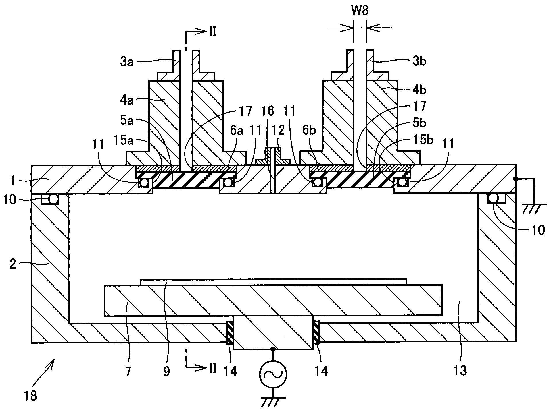
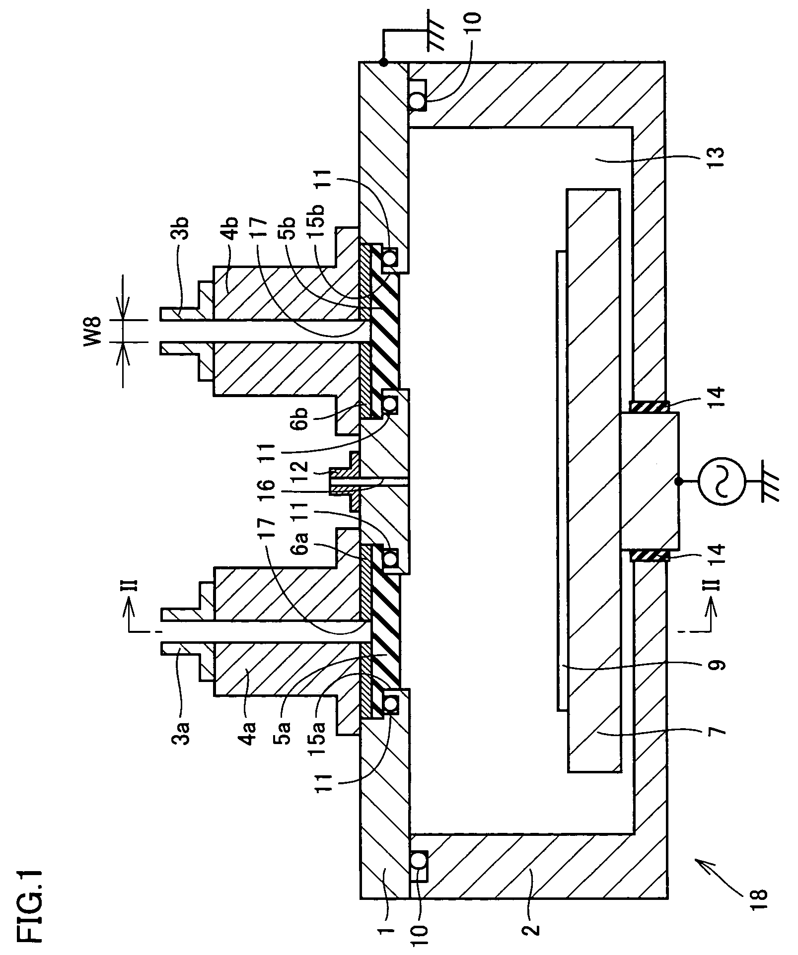
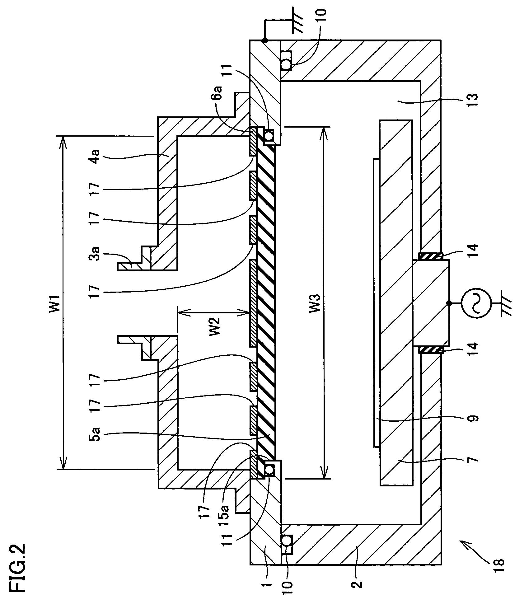
[0043]The first embodiment of the plasma processing apparatus according to the present invention is now described with reference to FIGS. 1-3.
[0044]Referring to FIGS. 1-3, the plasma processing apparatus 18 is a processing apparatus for performing plasma processing such as film deposition, etching or the like using plasma. Plasma processing apparatus 18 includes a process chamber body 2 made of a member of aluminum or aluminum having coating thereon, a chamber lid 1 arranged on top of process chamber body 2, lead-in waveguides 4a and 4b arranged on top of chamber lid 1, and waveguides 3a and 3b connected to lead-in waveguides 4a and 4b, respectively. Process chamber body 2 and chamber lid 1 constitute a chamber as the processing chamber. A substrate holder 7 for holding a substrate 9 to be processed is arranged in the chamber interior 13. Substrate holder 7 is made of a conductor such as a metal. A stand for supporting substrate holder 7 is provided beneath substrate holder 7. The s...
second embodiment
[0076]The second embodiment of the plasma processing apparatus according to the present invention is now described with reference to FIG. 5, which corresponds to FIG. 2.
[0077]Referring to FIG. 5, the plasma processing apparatus 18 has a structure basically similar to that of the plasma processing apparatus shown in FIGS. 1-3, except for the number and arrangement of dielectrics 19a, 19b. In plasma processing apparatus 18 shown in FIG. 5, two openings 20a, 20b are formed at chamber lid 1 in a region beneath lead-in waveguide 4a, along a longitudinal direction of lead-in waveguide 4a. Dielectrics 19a and 19b are fitted in openings 20a and 20b, respectively. Dielectrics 19a, 19b each have a rectangular shape in cross section in a direction approximately perpendicular to the microwave radiating direction. Similarly, two openings are formed at chamber lid 1 beneath lead-in waveguide 4b (see FIG. 1). Dielectrics having identical shapes to those of dielectrics 19a, 19b of FIG. 5 are fitted...
examples
[0081]To confirm the simulated results in the second embodiment described above, two kinds of samples of dielectrics, having thicknesses T of 15.0 mm and 27.5 mm respectively, were prepared as dielectrics 19a, 19b in the plasma processing apparatus shown in FIG. 5. The dielectric samples were placed in plasma processing apparatus 18 separately, and breakdown voltage values were measured. For simulation of the reactant gas, an argon (Ar) gas was supplied to chamber interior 13 at a flow rate of 500 sccm (0.5 l / min) to cause discharge. The results are shown in FIG. 7.
[0082]Referring to FIG. 7, the horizontal axis represents a gas pressure of the chamber interior, and the vertical axis represents a microwave power. The solid line represents the lower limit of discharge range (condition range enabling plasma generation) when thickness T of dielectrics 19a, 19b is 15.0 mm. The broken line represents the lower limit of discharge range when thickness T of dielectrics 19a, 19b is 27.5 mm.
[0...
PUM
| Property | Measurement | Unit |
|---|---|---|
| pressure | aaaaa | aaaaa |
| frequency | aaaaa | aaaaa |
| distance | aaaaa | aaaaa |
Abstract
Description
Claims
Application Information


