Solder interconnect integrity monitor

a solder interconnect and integrity monitor technology, applied in the field of packaging integrated circuits, can solve the problems of increased clock speed, increased power consumption, and increased integration, and achieve the effect of increasing the number of inputs and outputs, increasing the integration rate, and increasing the clock speed

Active Publication Date: 2009-01-20
ORACLE INT CORP
View PDF8 Cites 15 Cited by
  • Summary
  • Abstract
  • Description
  • Claims
  • Application Information

AI Technical Summary

Benefits of technology

[0013]In accordance with the present invention, the method and apparatus for monitoring solder interconnect package connections is set forth, which provides a non-destructive method of detecting brittle solder joint fractures, as they...

Problems solved by technology

Integrated circuit technology continues to evolve, resulting in chips with increased clock speeds, higher power consumption, and larger numbers of inputs and outputs.
Corresponding advances in integrated circuit fabrication technology have resulted in higher levels of integration, increased density, and growth in die sizes, any or all of which can pose additional challenges when packaging and mounting semiconductor devices.
A fundamental problem in semiconductor package mounting is brittle solder joint fractures.
Unlike fatigue failures, these fractures typically occur during a monotonic (non-reversing) stress event such as drop or high strain rate flexure.
For example, in-circuit test (ICT) and certain assembly operations, such as manual connector insertion and printed wire board (PWB) edge-guide snap-off, are often associated with high strain and strain-rate.
Such operations can also result in high PWB flexural loading, depending upon system configuration, assembly location, and other factors.
Although they occur infrequently, brittle solder interconnect fractures are nonetheless a major concern given the possibility of undetected failures.
Some brittle solder joint fractures may be detected prior to shipment, while others may go undetected due to e...

Method used


Image

  • Solder interconnect integrity monitor
  • Solder interconnect integrity monitor
  • Solder interconnect integrity monitor

Examples


Embodiment Construction

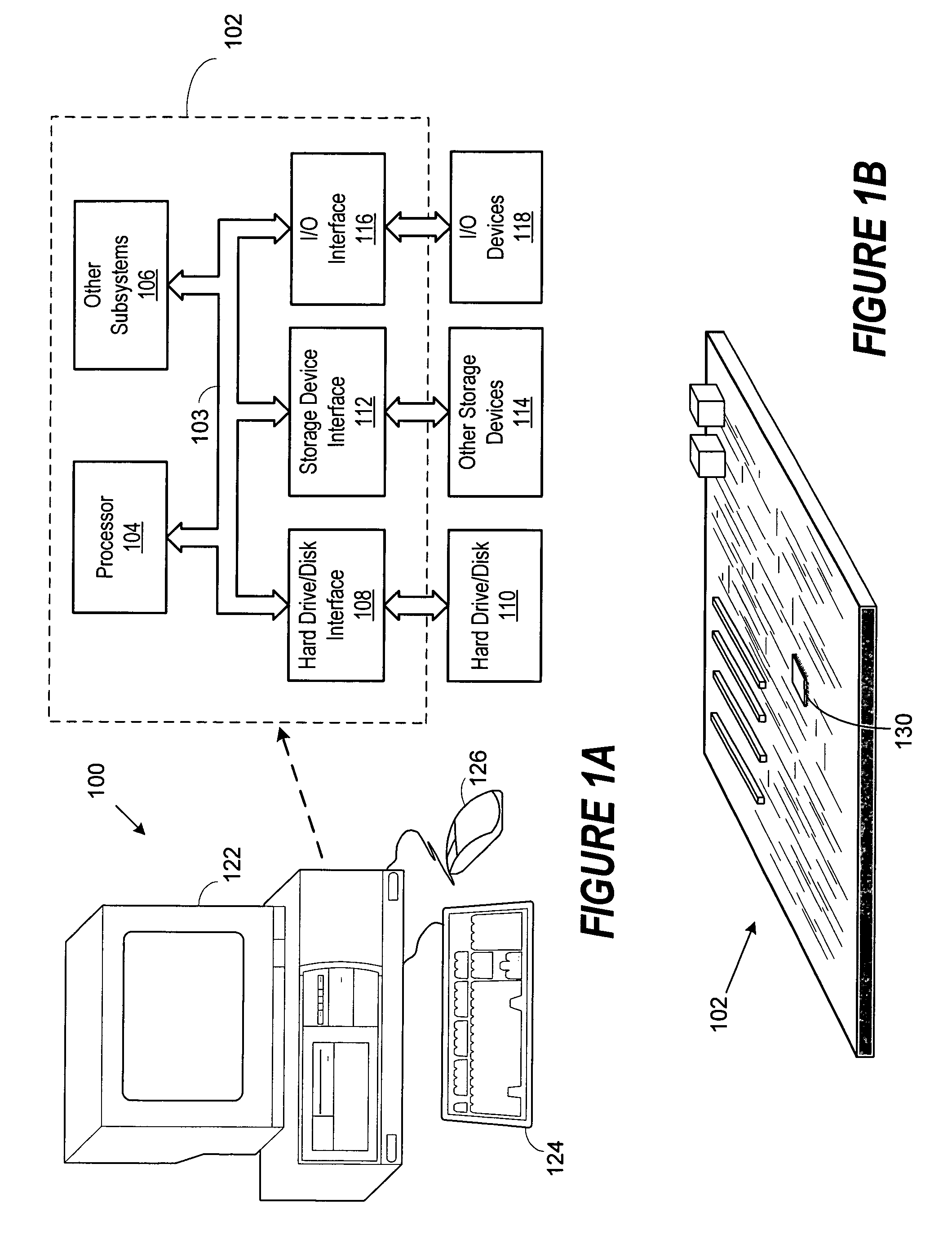
[0032]The method and apparatus of the present invention provides significant improvements in the electronic devices such as those used in a computer system 100 shown in FIG. 1A. The computer system 100 includes a main system board 102 that comprises a plurality of integrated circuits, such as a processor 104 and integrated circuits used for various other subsystems 106 understood by those skilled in the art. Data is transferred between the various system components via various data buses illustrated generally by bus 103. A hard drive 110 is controlled by a hard drive / disk interface 108 that is operably connected to the hard drive / disk 110. Likewise, data transfer between the system components and other storage devices 114 is controlled by storage device interface 112 that is operably connected to the various other storage devices 114, such as CD ROM drives, floppy drives, etc. An input / output (I / O) interface 118 controls the transfer of data between the various system components and...


PUM

PropertyMeasurementUnit
Stress optical coefficientaaaaaaaaaa
Strain pointaaaaaaaaaa
Electrical currentaaaaaaaaaa

Abstract

An apparatus and method for non-destructive solder interconnect integrity monitoring that can detect existing fracture damage, identify new or incipient fractures, and be implemented across multiple component configurations. Said components can be implemented to detect, on a continuous basis, solder interconnect fractures as they occur during actual end-use, throughout the lifecycle of monitored components, rather than relying on a one-time electrical check prior to shipment.

Description

BACKGROUND OF THE INVENTION[0001]1. Field of the Invention[0002]The present invention relates in general to the field of packaging integrated circuits, and more specifically, to detecting solder interconnect fractures as they occur during the lifecycle of monitored components.[0003]2. Description of the Related Art[0004]Integrated circuit technology continues to evolve, resulting in chips with increased clock speeds, higher power consumption, and larger numbers of inputs and outputs. Corresponding advances in integrated circuit fabrication technology have resulted in higher levels of integration, increased density, and growth in die sizes, any or all of which can pose additional challenges when packaging and mounting semiconductor devices.[0005]A semiconductor device is an integrated circuit in packaged form, usually mounted to a printed wire board (PWB) or other type of carrier, operating as a processing unit, memory, controller or any other electronic device. Semiconductor package...

Claims


Application Information

Patent Timeline
IPC IPC(8): B23K31/12
CPCB23K31/12G01R31/048H01L22/14H05K1/0268H05K3/3436H01L2924/014H01L2924/15162H01L2924/0002H05K3/3463H05K2201/094H05K2203/163H01L2924/00G01R31/71Y02P70/50
Inventor NEWMAN, KEITH G.
Owner ORACLE INT CORP
Why Eureka
Try Eureka