
Multiwalled carbon nanotube memory device

Inactive Publication Date: 2009-01-27
IBM CORP
View PDF2 Cites 14 Cited by
  • Summary
  • Abstract
  • Description
  • Claims
  • Application Information

AI Technical Summary

Problems solved by technology

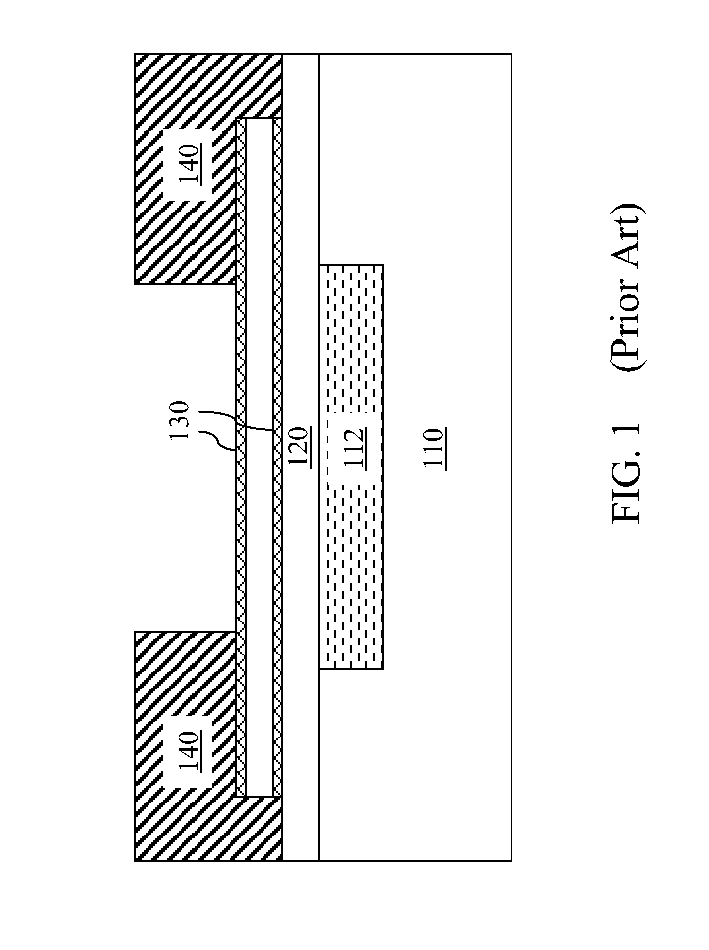
While some prototype semiconductor devices employing carbon nanotubes have been proposed as described above, the variety of available semiconductor devices based on carbon nanotubes is limited.

Method used


Image

  • Multiwalled carbon nanotube memory device
  • Multiwalled carbon nanotube memory device
  • Multiwalled carbon nanotube memory device

Examples


Embodiment Construction

[0063]As stated above, the present invention relates to a multiwall carbon nanotube memory device and methods of manufacturing the same, which are now described in detail with accompanying figures. It is noted that like and corresponding elements are referred to by like reference numerals.

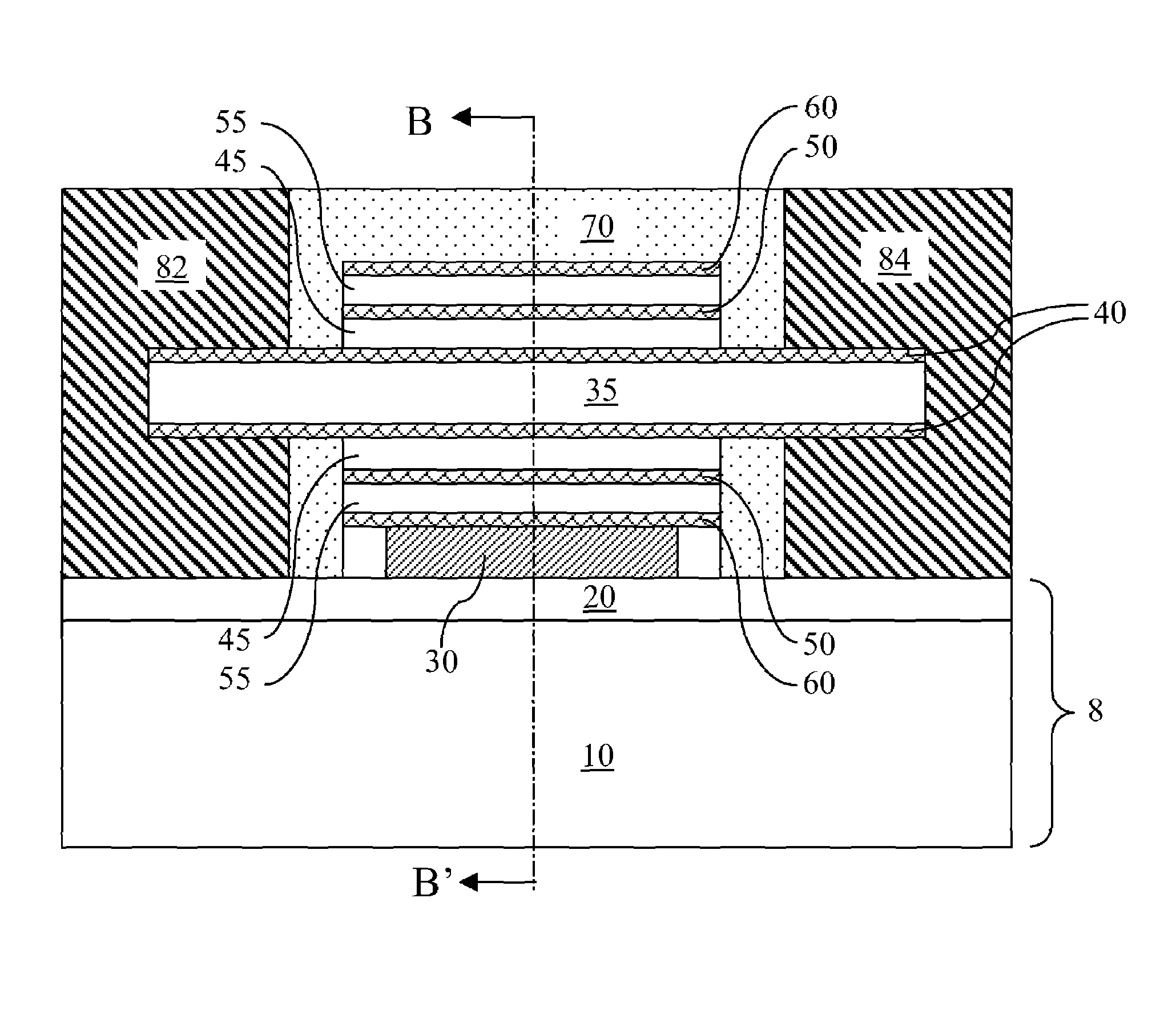
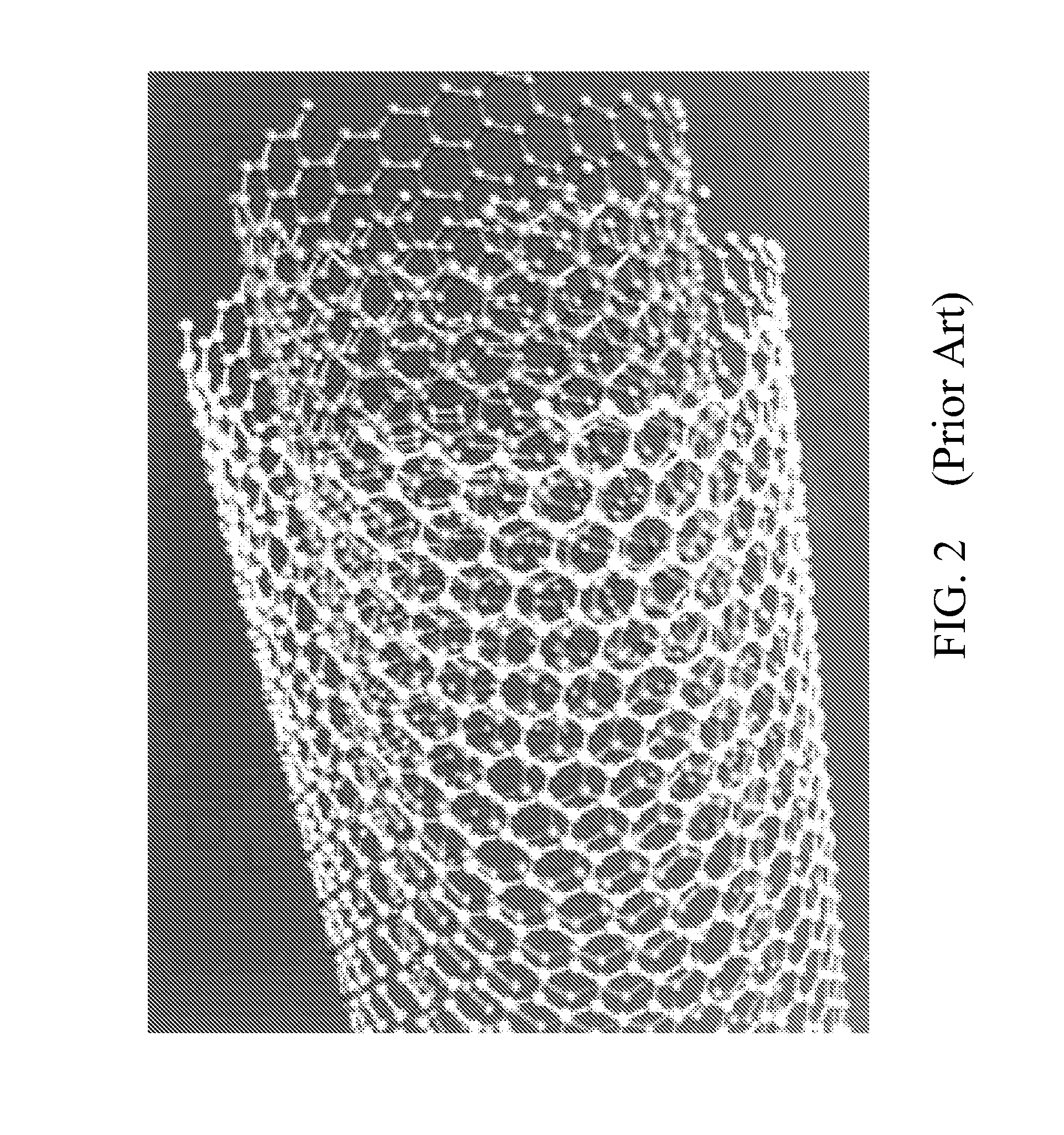
[0064]Referring to FIG. 4, a set of three concentric carbon nanotubes is shown, which is employed to form a carbon nanotube structure according to the present invention. The set of three carbon nanotubes comprises an inner carbon nanotube 40 having a first diameter d1, a middle carbon nanotube 50 having a second diameter d2, and an outer carbon nanotube 60 having a third diameter d3. The first diameter d1 is from about 1.0 nm to about 40 nm, and preferably from about 1.3 nm to about 10 nm, and more preferably from about 1.7 nm to about 4.0 nm. Preferably, the inner carbon nanotube 40 is semiconducting.

[0065]The second diameter d2 is greater than the first diameter d1, and the third diameter d3 is g...


PUM


Abstract

A carbon nanotube based memory device comprises a set of three concentric carbon nanotubes having different diameters. The diameters of the three concentric carbon nanotubes are selected such that an inner carbon nanotube is semiconducting, and intershell electron transport occurs between adjacent carbon nanotubes. Source and drain contacts are made to the inner carbon nanotube, and a gate contact is made to the outer carbon nanotube. The carbon nanotube based memory device is programmed by storing electrons or holes in the middle carbon nanotube through intershell electron transport. Changes in conductance of the inner carbon nanotube due to the charge in the middle shell are detected to determine the charge state of the middle carbon nanotube. Thus, the carbon nanotube based memory device stores information in the middle carbon nanotube in the form of electrical charge.

Description

FIELD OF THE INVENTION[0001]The present invention relates to a carbon nanotube structure, and particularly to a multiwalled carbon nanotube memory device and methods of manufacturing the same.BACKGROUND OF THE INVENTION[0002]As scaling for conventional CMOS integrated circuits approaches quantum mechanical limits, alternative nanostructures and materials have been investigated in the semiconductor industry. Of such nanostructures and materials, carbon nanotubes (CNTs) offer excellent intrinsic properties that are suitable for high performance nanoscale devices.[0003]A key advantage of CNTs over conventional CMOS devices is that scaling limitations of MOSFETs due to boundary scattering of electrons from imperfect interfaces are solved naturally in CNTs which have a smooth, well coordinated graphene structure with no bonds to the outside. This enables CNTs to retain excellent transport properties to much smaller lateral dimensions than silicon. The small radius and possibility of comp...

Claims


Application Information

Patent Timeline
IPC IPC(8): H01L21/00
CPCB82Y10/00G11C13/025H01L29/0665H01L29/0673H01L29/1606H01L51/0558G11C16/0416G11C2213/17H01L21/28273H01L51/0048Y10S977/742Y10S977/939H01L29/40114H10K85/221H10K10/484
Inventor YANG, HAINING S.
Owner IBM CORP
Learn More