3D IC method and device

a three-dimensional integrated circuit and integrated circuit technology, applied in the field of three-dimensional integrated circuits, can solve the problems of increasing ic cost, reducing chip yield, and reducing yield

Active Publication Date: 2009-02-03
INVENSAS BONDING TECH INC
View PDF16 Cites 384 Cited by
  • Summary
  • Abstract
  • Description
  • Claims
  • Application Information

AI Technical Summary

Problems solved by technology

The realization of these applications in a single, large area IC die typically results in a reduction in chip yield and, correspondingly, increased IC cost.
This increase in mask levels typically also results in a reduction in yield, and correspondingly, increased IC cost.
The cost of the vertical interconnection portion of this approach is directly related to the number of photolithography masking levels required to etch vias and form electrical interconnects.
This results in a patterning over a non-planar structure that limits the scaling of the structure to very small feature size that is desirable to achieve the highest interconnection density and consumes the least possible silicon substrate where functional transistors would otherwise reside.

Method used


Image

  • 3D IC method and device
  • 3D IC method and device
  • 3D IC method and device

Examples


first embodiment

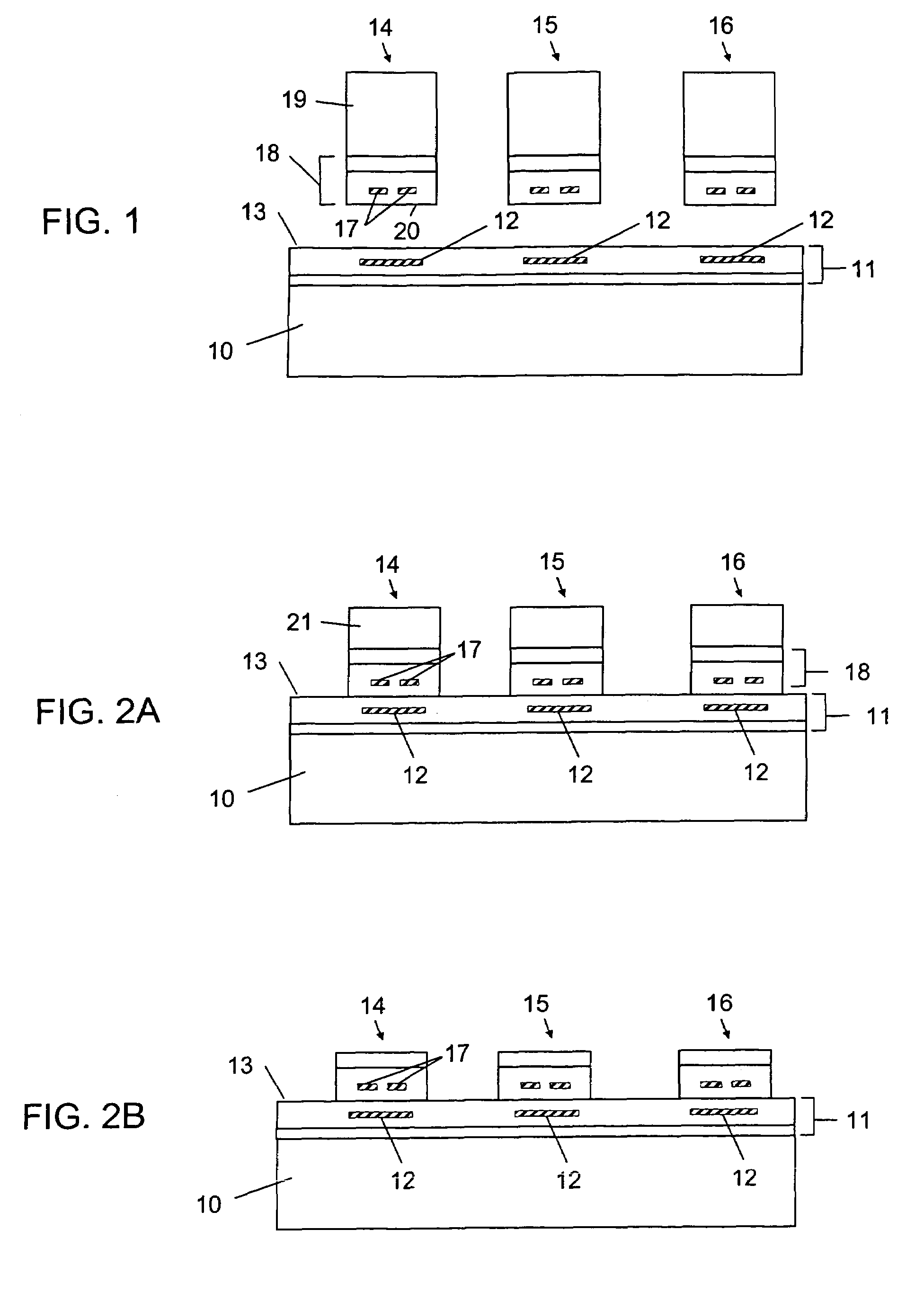
[0063]Referring now to the drawings, in particular FIG. 1, the method according to the invention will be described. It is noted here that the drawings are not drawn to scale but are drawn to illustrate the concepts of the invention.

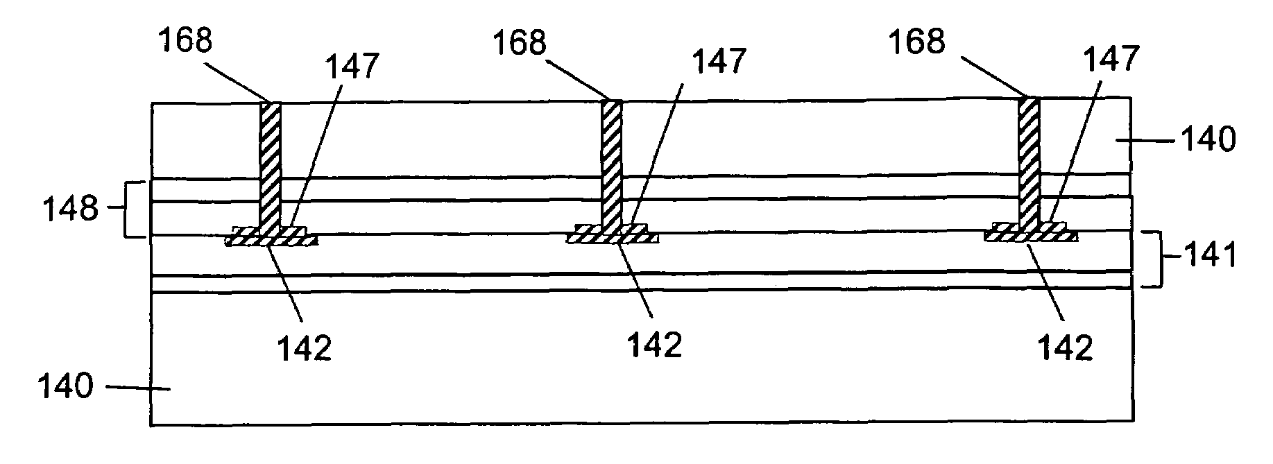
[0064]Substrate 10 includes a device region 11 having contact structures 12. Substrate 10 may be made of a number of materials, such as semiconductor material or insulating material, depending on the desired application. Typically, substrate 10 is made of silicon or III-V materials. Contact structures 12 are typically metal pads or interconnect structures making contact to device or circuit structures (not shown) formed in substrate 10. Substrate 10 may also contain an integrated circuit to which the contact structures 12 are connected, and substrate 10 may be a module containing only contact structures. For example, substrate 10 may be a module for interconnecting structures bonded to substrate 10, or bringing out connections for packaging or integration...

fourth embodiment

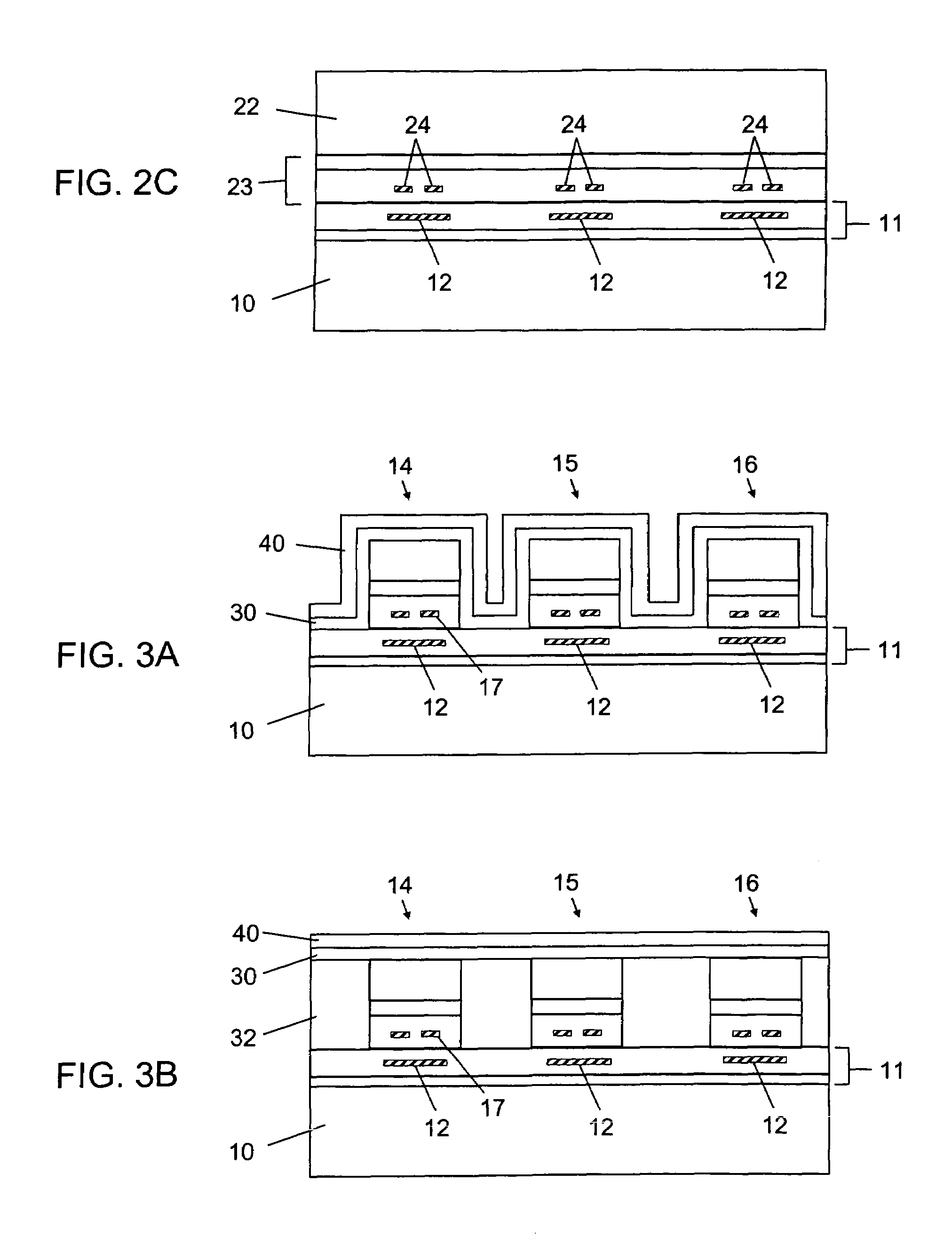
[0067]An additional factor that determines the optimum size of the gap or aperture is a ratio of a distance given by the vertical separation between contact structures 17 and 12 plus the thickness of the contact structure 17 to the size of the gap or aperture. This defines an aspect ratio of a via that will subsequently be formed between contact structures 17 and 12 to enable an electrical interconnection between contact structures 17 and 12. This vertical separation is typically 1-5 microns, or less, for oxide to oxide direct bonding, as described in application Ser. No. 09 / 505,283, the contents of which are incorporated herein by reference, or potentially zero for metal direct bonding, as described in application Ser. No. 10 / 359,608, the contents of which are herein incorporated by reference. Furthermore, the contact structure 17 thickness is typically 0.5 to 5 microns. With a typical desired via aspect ratio of 0.5 to 5 depending on the process technology used, a typical range of...

fifth embodiment

[0113]A fifth embodiment is shown in FIGS. 20A-20H. This embodiment is similar to the previous embodiments before the formation of via 50 with the exception that contact structures in die 17, 108, 117, or 123 with an aperture or edge that overlaps via 50 is replaced with contact structure 87 without an aperture or overlapping edge. In this embodiment, contact structures 87 in die 84-86 with substrate portion 89, device region 88 are bonded to surface 83 with device region 81, substrate 80, and contact structures 82. Contact structure 87 is positioned over contact structure 82 as shown in FIG. 20A. Die 84-86 can also be bonded to a surface 113 with exposed contact structures 112 similar to that shown in FIGS. 16 and 17 or contact structures 122 similar to that shown in FIGS. 18 and 19. Note that the contact structure 87 may be bonded in direct contact with contact structure 82, which is illustrated in device 86. Dies 84-86 may also have the same contact structure configuration. FIGS....


PUM


Abstract

A method of three-dimensionally integrating elements such as singulated die or wafers and an integrated structure having connected elements such as singulated dies or wafers. Either or both of the die and wafer may have semiconductor devices formed therein. A first element having a first contact structure is bonded to a second element having a second contact structure. First and second contact structures can be exposed at bonding and electrically interconnected as a result of the bonding. A via may be etched and filled after bonding to expose and form an electrical interconnect to interconnected first and second contact structures and provide electrical access to this interconnect from a surface. Alternatively, first and / or second contact structures are not exposed at bonding, and a via is etched and filled after bonding to electrically interconnect first and second contact structures and provide electrical access to interconnected first and second contact structure to a surface. Also, a device may be formed in a first substrate, the device being disposed in a device region of the first substrate and having a first contact structure. A via may be etched, or etched and filled, through the device region and into the first substrate before bonding and the first substrate thinned to expose the via, or filled via after bonding.

Description

CROSS-REFERENCE TO RELATED APPLICATIONS[0001]This application is related to applications Ser. No. 09 / 532,886, now U.S. Pat. No. 6,500,794, Ser Nos. 10 / 011,432, 10 / 359,608, 10 / 688,910, now U.S. Pat. No. 6,867,073, and Ser. No. 10 / 440,099, the entire contents of which are incorporated herein by reference.BACKGROUND OF THE INVENTION[0002]1. Field of the Invention[0003]The present invention relates to the field of three-dimensional integrated circuits and more particularly to devices and the fabrication thereof of three-dimensional integrated circuits using direct wafer bonding.[0004]2. Description of the Related Art[0005]Semiconductor integrated circuits (ICs) are typically fabricated into and on the surface of a silicon wafer resulting in an IC area that must increase as the size of the IC increases. Continual improvement in reducing the size of transistors in ICs, commonly referred to as Moore's Law, has allowed a substantial increase in the number of transistors in a given IC area. ...

Claims


Application Information

Patent Timeline
Patent Type & Authority Patents(United States)
IPC IPC(8): H01L23/48
CPCH01L21/76898H01L23/481H01L24/02H01L24/81H01L24/94H01L24/97H01L25/0657H01L25/50H01L21/76838H01L2224/81121H01L2224/81201H01L2224/8123H01L2224/81801H01L2224/81894H01L2224/83894H01L2224/9202H01L2224/97H01L2225/06513H01L2225/06541H01L2924/01002H01L2924/01004H01L2924/01005H01L2924/01007H01L2924/01013H01L2924/01014H01L2924/01015H01L2924/01018H01L2924/0102H01L2924/01022H01L2924/01027H01L2924/01028H01L2924/01029H01L2924/01033H01L2924/01042H01L2924/01046H01L2924/01049H01L2924/0105H01L2924/01059H01L2924/01073H01L2924/01074H01L2924/01075H01L2924/01077H01L2924/01078H01L2924/01079H01L2924/01082H01L2924/014H01L2924/04941H01L2924/04953H01L2924/05042H01L2924/10329H01L2924/12044H01L2924/14H01L2924/19043H01L2924/3025H01L2224/81H01L2924/01006H01L2924/01019H01L2924/01023H01L2924/01055H01L2224/81931H01L2224/0401H01L2224/9212H01L24/82H01L24/80H01L24/92H01L24/24H01L24/08H01L2224/08225H01L2224/24225H01L2224/80001H01L2224/82H01L21/4763H01L23/12H01L27/0688
Inventor ENQUIST, PAUL M.FOUNTAIN, JR., GAIUS GILLMANTONG, QIN-YI
Owner INVENSAS BONDING TECH INC
Why Eureka
Try Eureka