Method for detecting and monitoring defects

a technology of defect detection and monitoring method, applied in the field of statistical process control method, can solve the problems of low level defects, devices ultimately formed with the interconnects that fall outside the tolerance range will be defective, and the resistance measurement is generally not sensitive enough to detect small defects

Active Publication Date: 2009-02-03
CHARTERED SEMICONDUCTOR MANUFACTURING
View PDF23 Cites 15 Cited by
  • Summary
  • Abstract
  • Description
  • Claims
  • Application Information

AI Technical Summary

Problems solved by technology

Likewise, if the thickness of the film layer is substantially non-uniform, the electrical resistance of a potion of the interconnects will fall outside of the desired tolerance range.
In these cases, the devices ultimately formed with the interconnects that fall outside of the tolerance range will be defective.
However, the inventor has found resistance measurements are generally not sensitive enough to detect small, low level defects, such as void defects.
These techniques become less effective, however, as geometries continue to shrink into the deep submicron regime, since the size for which defects are critical also shrink.
Defects such as interior voids in conductive lines are even more difficult to detect visually.
Moreover, some defects, such as stress induced voids in Al lines, may not appear until several process steps after the Al conductors were inspected.

Method used


Image

  • Method for detecting and monitoring defects
  • Method for detecting and monitoring defects
  • Method for detecting and monitoring defects

Examples


examples

[0089]The following non-limiting examples represent preferred forms and best modes contemplated by the inventor for practice of his invention, as well as illustrating the results obtained through its use.

[0090]A. Resistance Test—

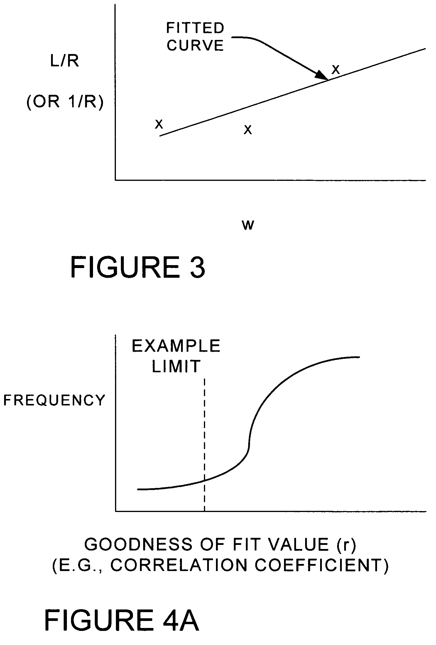
[0091]Below is an example of an embodiment of the invention simulated for a resistance measurement of test structure on a integrated circuit. The simulation is for 30 long lines, divided into 30 individual segments of 1 μm.

[0092]The electrical resistance of a line or wire is well known to be:

R=ρ(L / A)  (1)

where:[0093]ρ is the resistivity[0094]L is the resistor / conductor length[0095]A is the cross-sectional area

For a rectangular cross-section,

A=W*T  (2)

with:[0096]A=area[0097]W being the resistor width[0098]T being the height or thickness

In the case of a thin film, the resistance equation is often expressed as:

R=Rs(L / W)  (3)

with[0099]R is resistance[0100]Rs, known as sheet resistance, then defined as:

Rs=ρ / T  (4)

and the ratio of length to width, L / W, is often re...


PUM


Abstract

A method that uses a goodness of fit test / measurement (e.g., correction coefficient) for process control of a test parameter (e.g., resistance). At least the minimum number of test values required to calculate a goodness of fit test is obtained. A curve is fitted for the test parameters values and the independent variable(s). A goodness of fit measurement / test (e.g., correlation coefficient) is calculated for the curve and data. The goodness of fit measurement value is used for process control. Control limits can be established on the goodness of fit measurement values. The use of the goodness of fit test is a sensitive test that can used to control processes with low level defects or small fluctuations.

Description

BACKGROUND OF INVENTION[0001]1. Field of the Invention[0002]This invention relates generally to methods to control processes and to screen product and more particularly to a statistical process control method for using regression analysis and goodness of fit measurements to control processes and / or to screen devices and more particularly to a statistical process control method for using goodness of fit measurements to control electronic / semiconductor manufacturing processes, such as resistance and void defects in conductive lines.[0003]2. Description of the Prior Art[0004]During the fabrication of semiconductor devices, multiple film layers are deposited on a substrate. Preferably, the film layer should form a continuous coating of uniform thickness over the entire surface of the substrate. For example, a metal film layer may be used to cover a dielectric layer, wherein the dielectric layer includes holes or trenches extending therethrough. The metal film fills or conformally covers...

Claims


Application Information

Patent Timeline
Patent Type & Authority Patents(United States)
IPC IPC(8): G06F19/00G06F15/00G06F17/18H01L21/66
CPCH01L22/20H01L2924/0002H01L2924/00
Inventor LIM, SHELDON C. P.
Owner CHARTERED SEMICONDUCTOR MANUFACTURING
Why Eureka
Try Eureka