Wireless semiconductor device having low power consumption

a technology of semiconductor devices and wires, applied in the direction of power supply for data processing, liquid/fluent solid measurement, instruments, etc., can solve the problems of difficult stabilization of power, complex process of wireless tags, and power consumption that is required to be suppressed, so as to improve communication distance to readers/writers, low power consumption, and stable operation

Inactive Publication Date: 2009-02-03
SEMICON ENERGY LAB CO LTD
View PDF48 Cites 57 Cited by
  • Summary
  • Abstract
  • Description
  • Claims
  • Application Information

AI Technical Summary

Benefits of technology

[0006]In view of the foregoing, the invention provides a semiconductor device in which stabilization of power is achieved by suppressing the power consumption as much as possible. In addition, the invention provides a semiconductor device in which power is not unstable due to a complex process such as a cryptanalysis and stabilization of the power is achieved. Furthermore, the invention provides a semiconductor device in which strong electromagnetic waves are not required to be input and the communication distance to a reader / writer is improved.
[0011]According to the invention having the above-described constitution, a semiconductor device in which low power consumption is achieved can be provided. Therefore, such a semiconductor device can be provided that power is not unstable due to a complex process such as a cryptanalysis and stable operation is achieved. In addition, such a semiconductor device can be provided that strong electromagnetic waves are not required to be input and the communication distance to a reader / writer is improved.

Problems solved by technology

In a wireless tag, power is difficult to be stabilized and power consumption is required to be suppressed as much as possible because the power is supplied from an antenna.
In addition, a wireless tag carries out complex processes such as reading out data from a storage medium and a cryptanalysis.
In order to carry out such a complex process as the cryptanalysis, there has been a problem that high power consumption has been required.
As the power consumption is increased, strong electromagnetic waves are required to be input, there has been a problem that high power consumption of a reader / writer has been needed and other device and the human body have been adversely affected, for example.
Furthermore, the communication distance between the wireless tag and the reader / writer has been restricted.

Method used


Image

  • Wireless semiconductor device having low power consumption
  • Wireless semiconductor device having low power consumption
  • Wireless semiconductor device having low power consumption

Examples


embodiment 1

[0032]Constitution of the operation-frequency detecting means and the discriminating means in the detecting portion 13 is described using FIGS. 4A and 4B. The operation-frequency detecting means includes an address comparator 71, an address memory 72, a counter 73, and a reset signal generating circuit 74. The discriminating means includes a discriminating circuit 75 and a discriminating reference data memory 76.

[0033]The address comparator 71 is connected to an address bus 70 and the address memory 72. First address data is input from the address bus 70. The first address data and second address data which is input to the address memory 72 are compared with each other by the address comparator 71. When the first address data and the second address data agree with each other, a signal showing the agreement is output to the counter 73. The counter 73 counts an output of the address comparator 71. The reset signal generating circuit 74 outputs a reset signal periodically to the counte...

embodiment 2

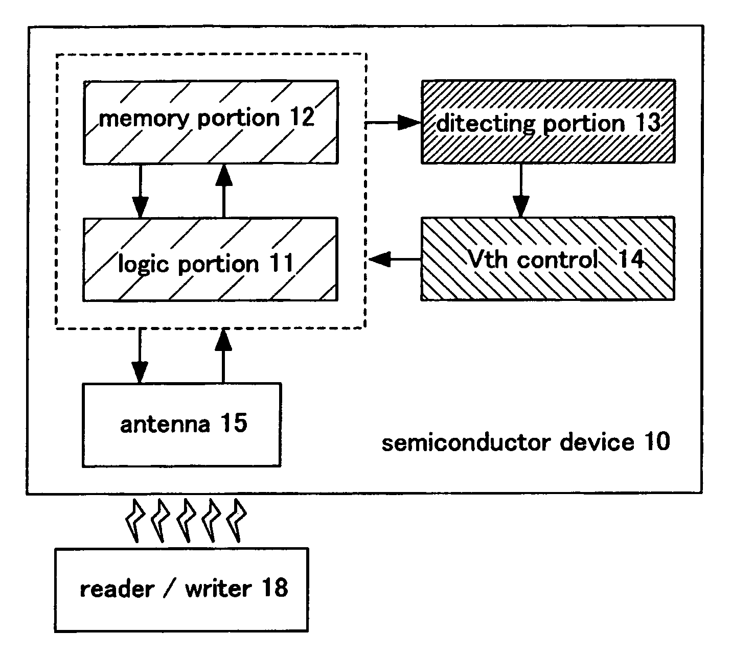
[0041]Constitution of the logic portion 11, which is one of the above-mentioned five components of the invention (the logic portion 11, the memory portion 12, the detecting portion 13, the Vth control 14, and the antenna 15), is described in detail using FIG. 5. A semiconductor device corresponding to a CPU is illustrated for description here.

[0042]The semiconductor device corresponding to a CPU comprises a timing control 51, an instruction decoder 52, a register array 53, an address logic and buffer 54, a data bus interface 55, an ALU (Arithmetic Logic Unit) 56, an instruction register 57, the detecting portion 13, and the Vth control 14. The timing control 51, for example, receives an instruction from the outside and converts it into data for the inside to transmit to another block, and provides an instruction of reading or writing of memory data, or the like to the outside depending on the inside operation. The instruction decoder 52 converts an outside instruction into an instru...

embodiment 3

[0044]According to a semiconductor device of the invention, data reading and data writing can be performed in a noncontact manner, and any one of data transmission methods can be employed which are generally classified into three methods, that is, an electromagnetic coupling method by which data communication is performed by mutual induction by a couple of coils being provided so as to face each other, an electromagnetic induction method by which data communication is performed by an induction electromagnetic field, and a radio wave method by which data communication is performed by utilizing radio waves. The antenna 15 for transmitting data is provided in two manners, that is, the case where the antenna 15 is provided over the substrate 20 having a plurality of transistors (see FIGS. 6A and 6C), and the case where a terminal portion is provided over the substrate 20 having a plurality of transistors and the antenna 15 is provided to connect to the terminal portion (see FIGS. 6B and...


PUM


Abstract

The invention provides a semiconductor device that power is stabilized by suppressing power consumption as much as possible. The semiconductor device of the invention includes a logic portion and a memory portion each including a plurality of transistors, a detecting portion for detecting one or both of operation frequencies of the logic portion and the memory portion, a Vth control for supplying a Vth control signal to one or both of the logic portion and the memory portion, and an antenna. Each of the plurality of transistors has a first gate electrode which is input with a logic signal, a second gate electrode which is input with the Vth control signal, and a semiconductor film such that the second gate electrode, the semiconductor film, and the first gate electrode are provided in this order from the bottom.

Description

TECHNICAL FIELD[0001]The present invention relates to a semiconductor device capable of transmitting and receiving data.BACKGROUND ART[0002]In recent years, a semiconductor device has been developed and used as a CPU and a memory. Among them, a semiconductor device which consumes large power has a problem that a larger battery and a cooling fan are required, thereby the electronic apparatus itself is increased in size. In view of the foregoing, a composite semiconductor device is suggested, which has a structure where a wiring substrate and a package are attached to each other so as to satisfy high thermal conductivity and low elasticity.[Patent Document 1][0003]Japanese Patent Laid-Open No. 07-74282[0004]A semiconductor device capable of transmitting and receiving data has been developed, which is called a wireless tag, an RFID tag, or the like. The semiconductor device which has been put to practical use comprises an antenna and a circuit formed using a semiconductor substrate (an...

Claims


Application Information

Patent Timeline
Patent Type & Authority Patents(United States)
IPC IPC(8): G06F1/32H01L21/77H01L27/12H01L27/13
CPCH01L27/1214H01L27/13H01L27/1266
Inventor KOYAMA, JUN
Owner SEMICON ENERGY LAB CO LTD
Why Eureka
Try Eureka