Method for manufacturing circuit modules and circuit module

a manufacturing method and circuit technology, applied in the field of circuit modules, can solve the problems of difficult to provide cutting grooves having a very large depth, inconsistent quality, and reduced productivity, and achieve the effect of excellent shielding properties and easy manufacturing

Active Publication Date:
View PDF16 Cites 90 Cited by
  • Summary
  • Abstract
  • Description
  • Claims
  • Application Information

AI Technical Summary

Benefits of technology

[0011]To overcome the problems described above, preferred embodiments of the present invention provide a method for manufacturing circuit modules and a circuit module capable of being easily manufactured and having an excellent shielding property.

Problems solved by technology

Consequently, this leads to a problem that the productivity is decreased, and inconsistent quality often occurs.
However, in order to ensure the mechanical strength of the aggregate substrate when being filled with the conductive material, it is difficult to provide cutting grooves having a very large depth.
For this reason, it is difficult to use a wiring substrate having a very small thickness, and this causes the side surfaces of the wiring substrate to have portions on which no shielding layer is formed.
Thus, a problem occurs in that it is difficult to obtain a sufficient shielding property.
As in Japanese Unexamined Patent Application Publication No. 2005-159227, it is not easy to precisely equalize the depth of cutting grooves to a depth corresponding to a height providing an exposure of ground electrodes formed on the surface of a wiring substrate.
There is a probability that the ground electrodes may be damaged or cut.
This causes the decrease in productivity.

Method used


Image

  • Method for manufacturing circuit modules and circuit module
  • Method for manufacturing circuit modules and circuit module
  • Method for manufacturing circuit modules and circuit module

Examples


first preferred embodiment

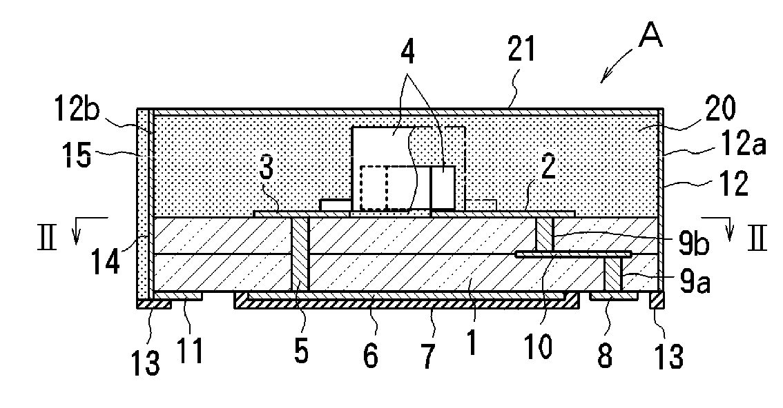
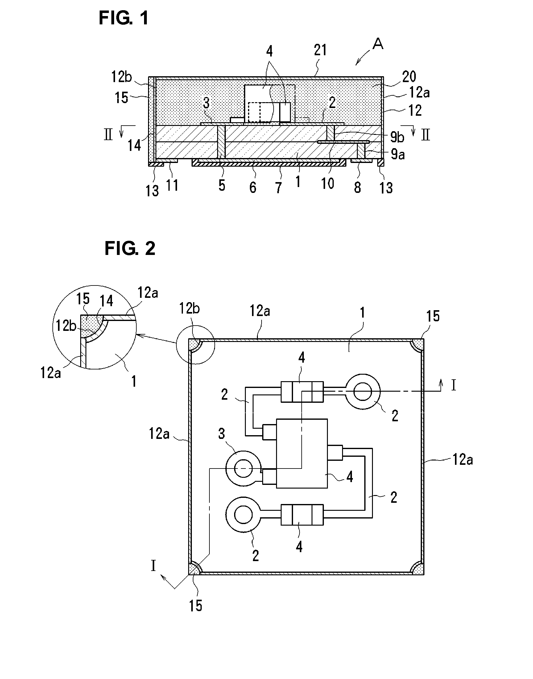
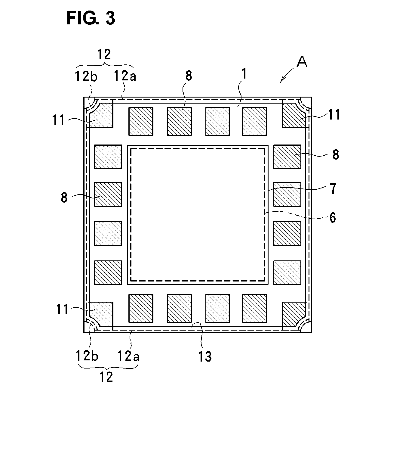
[0044]In FIGS. 1 to 3, a circuit module according to a first preferred embodiment of the present invention is shown. FIG. 1 is a sectional view taken along the step-formed cutting-plane line (the line I-I) of FIG. 2. FIG. 2 is a sectional view taken along the line II-II of FIG. 1. FIG. 3 is a bottom view.

[0045]A circuit module A includes a module substrate 1 that is a substrate having an insulating property, such as a multi-layered resin substrate, and that has a square or substantially square shape, for example. On the top surface of the module substrate 1, wiring electrodes 2, for example, used for inputs and outputs, and a ground electrode 3 are provided. To the electrodes 2 and 3, circuit components 4 including active components, such as transistors used for power amplifiers, and passive components, such as capacitors, are connected. The specific patterns of the wiring electrodes 2 and the ground electrode 3 shown in FIG. 2 are provided only as examples. Additionally, the circui...

second preferred embodiment

[0060]In FIGS. 6 to 8, a circuit module according to a second preferred embodiment is shown. The same elements as those according to the first preferred embodiment and elements corresponding to those according to the first preferred embodiment are denoted by the same reference numerals, and a description thereof is omitted. FIG. 6 is a sectional view taken along the step-formed cutting-plane line (the line VI-VI) of FIG. 7. FIG. 7 is a sectional view taken along the line VII-VII of FIG. 6. FIG. 8 is a bottom view.

[0061]In a circuit module B, electrode films 12c are formed along two opposed sides, and electrode films 12d are formed along the other two sides. The circuit module B is different from the circuit module A in that the side-surface-shielding layers 12 are defined by the electrode films 12c and 12b. Although the electrode films 12c are exposed to the outside, the electrode films 12d are covered by a filling material 30.

[0062]A method for manufacturing the circuit modules B a...

third preferred embodiment

[0070]In FIG. 10, a circuit module according to a third preferred embodiment is shown. The same elements as those according to the first preferred embodiment and elements corresponding to those according to the first preferred embodiment are denoted by the same reference numerals, and a description thereof is omitted. In the first preferred embodiment, after the electrode films 12b are formed on the inner surfaces of the first through holes 16, the first through holes 16 are filled with the filling material 15. However, in the third preferred embodiment, a filling material 40 composed of a conductive adhesive is used so that the filling material 40 can provide both functions.

[0071]Concave grooves 14 are formed in the corner portions of a circuit module C. The concave grooves 14 are filled with the filling material 40, which is composed of a conductive adhesive. The top and bottom ends of the filling material 40 are connected to the top-surface-shielding layer 21 and the ground termi...


PUM

PropertyMeasurementUnit
thicknessaaaaaaaaaa
conductiveaaaaaaaaaa
widthaaaaaaaaaa

Abstract

A module substrate defined by an aggregate substrate is prepared, and circuit components are mounted on the module substrate. An insulating resin layer is formed on substantially the entire top surface of the module substrate such that the circuit components are disposed in the insulating resin layer, and a top-surface-shielding layer is formed on the top surface of the insulating resin layer. First through holes are formed in the module substrate and the insulating resin layer at locations corresponding to portions of boundary lines of small substrates so as to extend in a thickness direction of the module substrate and the insulating resin layer. First electrode films are formed on the inner surfaces of the first through holes so as to be connected to the first shielding layer, and the first through holes are filled with a filling material. Next, second through holes are formed at locations corresponding to the remaining portions of the boundary lines of small substrates so as to extend in the thickness direction, and second electrode films are formed on the inner surfaces of the second through holes so as to be connected to the top-surface-shielding layer and the first electrode films. The filling material, with which the first through holes are filled, is cut along the boundary lines of small substrates, resulting in a division of the aggregate substrate into small substrates to obtain circuit modules.

Description

BACKGROUND OF THE INVENTION[0001]1. Field of the Invention[0002]The present invention relates to a circuit module in which a component-embedding substrate is used, and more particularly, the present invention relates to a circuit module having a function of an electromagnetic shield, and to a method for manufacturing such circuit modules.[0003]2. Description of the Related Art[0004]In the related art, circuit modules, such as voltage-controlled oscillators (VCOs) and antenna switches, are used in radio apparatuses, such as mobile phones, automobile telephones, and various types of communication apparatuses. A known circuit module has a configuration in which a leakage of an electromagnetic wave generated by a circuit component mounted on a module substrate can be avoided or in which the periphery of the circuit module is covered by shielding electrodes in order to block an electromagnetic wave that enters the circuit module from the outside.[0005]FIG. 12 shows an example of a circui...

Claims


Application Information

Patent Timeline
Patent Type & Authority Patents(United States)
IPC IPC(8): H05K9/00
CPCH01L21/561H01L23/552H01L24/97H01L25/0657H01L25/165H05K1/0218H05K3/403H01L23/3121Y10T29/49146H01L23/49822H01L23/49827H01L23/49833H01L25/162H01L2225/06541H01L2924/01004H01L2924/01029H01L2924/01033H01L2924/01074H01L2924/01078H01L2924/19041H01L2924/19043H01L2924/3025H05K3/0052H05K3/284H05K3/429H01L2924/01005H01L2924/01006H01L2924/014
Inventor KAWAGISHI, MAKOTOIEKI, TSUTOMU
Why Eureka
Try Eureka