High K stack for non-volatile memory

a non-volatile memory and dielectric constant technology, applied in the field of semiconductor devices, can solve the problems of affecting the device's overall performance and reliability, damage to the bottom oxide layer of the ono structure, etc., and achieves the effect of less damage, less charge loss, and convenient channel eras

Active Publication Date: 2009-02-17
MONTEREY RES LLC
View PDF35 Cites 0 Cited by
  • Summary
  • Abstract
  • Description
  • Claims
  • Application Information

AI Technical Summary

Benefits of technology

[0006]Consistent with aspects of the invention, a layer of dielectric material having a high dielectric constant may be formed over a top oxide layer in a semiconductor device, such as, for example, a non-volatile memory. The top oxide layer may be formed over a charge trapping layer that is further formed upon a bottom oxide layer. The dielectric constant of the layer of dielectric material may be greater than a dielectric constant of the bottom oxide layer. A gate electrode may be formed over the layer of high K dielectric material. Use of the layer of high K dielectric material facilitates channel erase in the semiconductor device which causes less damage to the bottom oxide layer, resulting in less charge loss and greater data retention reliability.

Problems solved by technology

BTBHH injection, however, causes damage to the bottom oxide layer of the ONO structure.
Over time, BTBHH-induced damage to the bottom oxide layer leads to data retention problems in the memory device and impairs the device's overall performance and reliability.

Method used


Image

  • High K stack for non-volatile memory
  • High K stack for non-volatile memory
  • High K stack for non-volatile memory

Examples


Embodiment Construction

[0018]The following detailed description of the invention refers to the accompanying drawings. The same reference numbers in different drawings may identify the same or similar elements. Also, the following detailed description does not limit the invention. Instead, the scope of the invention is defined by the appended claims and their equivalents.

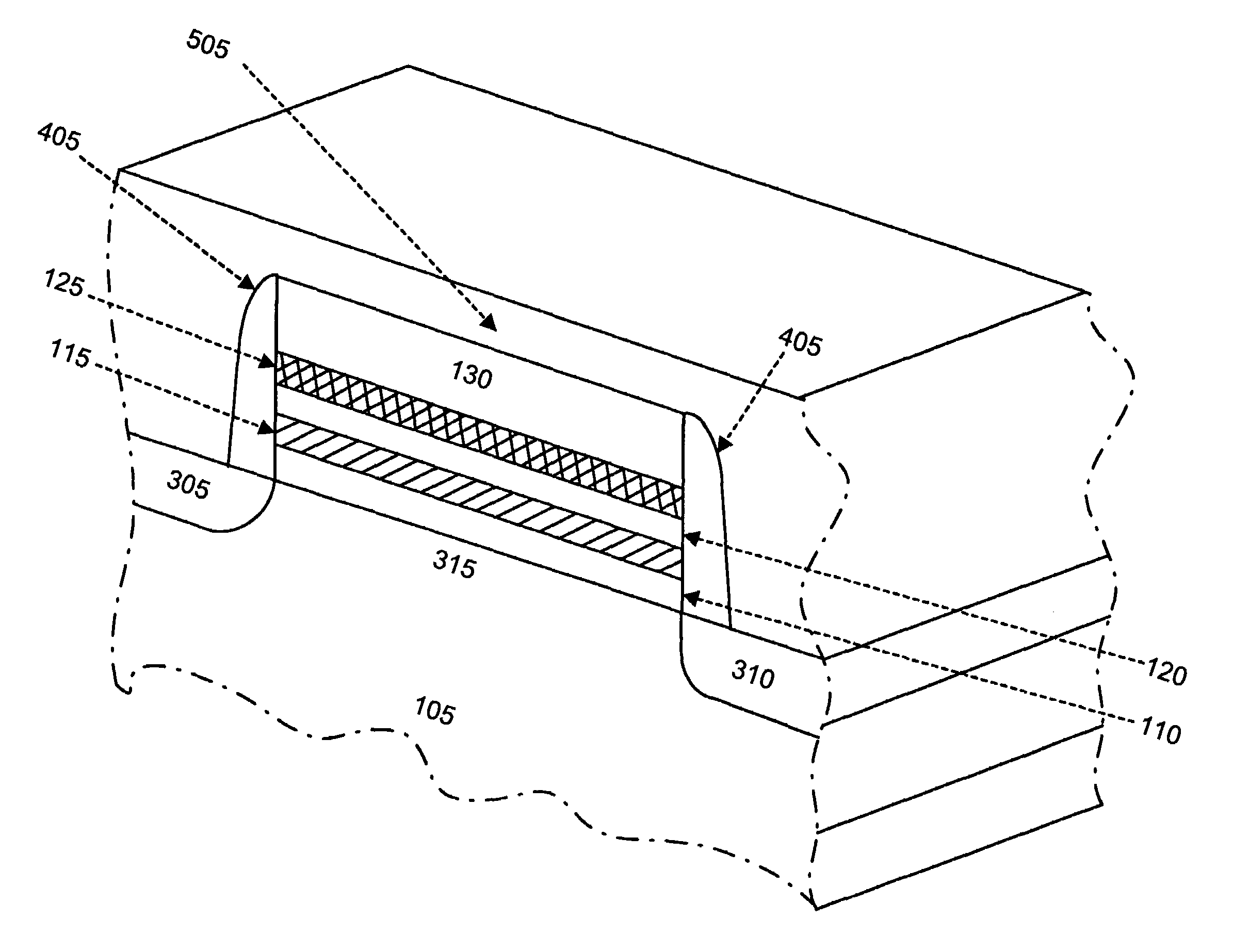
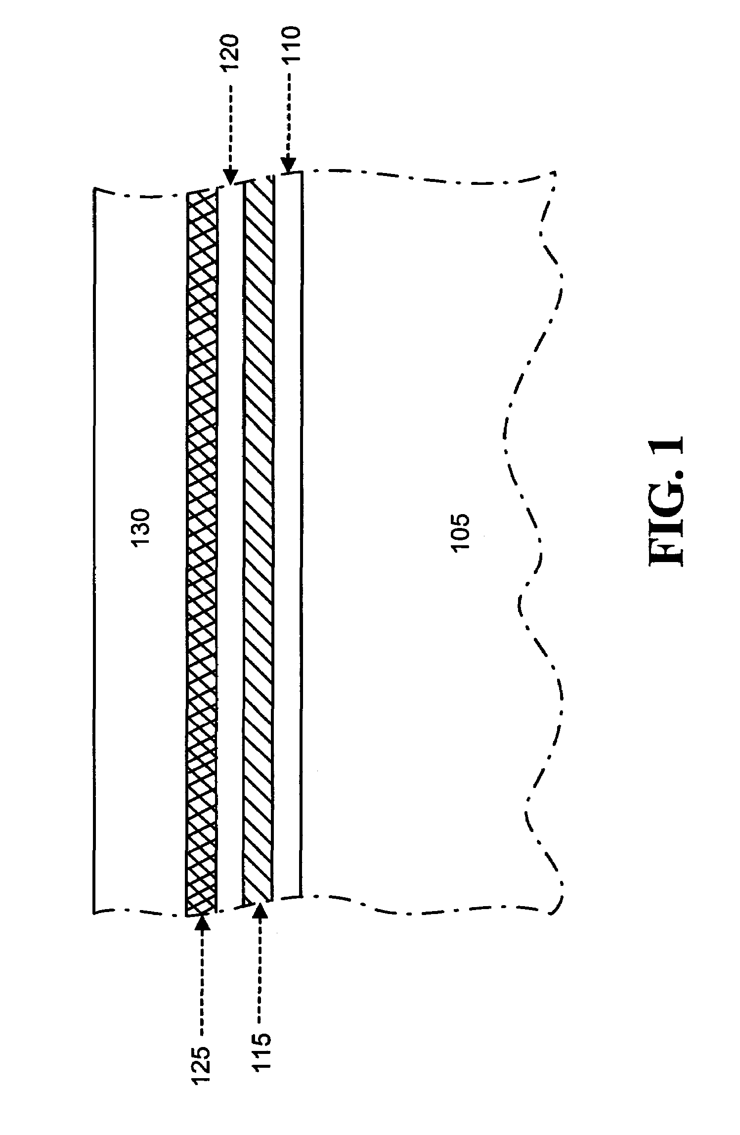
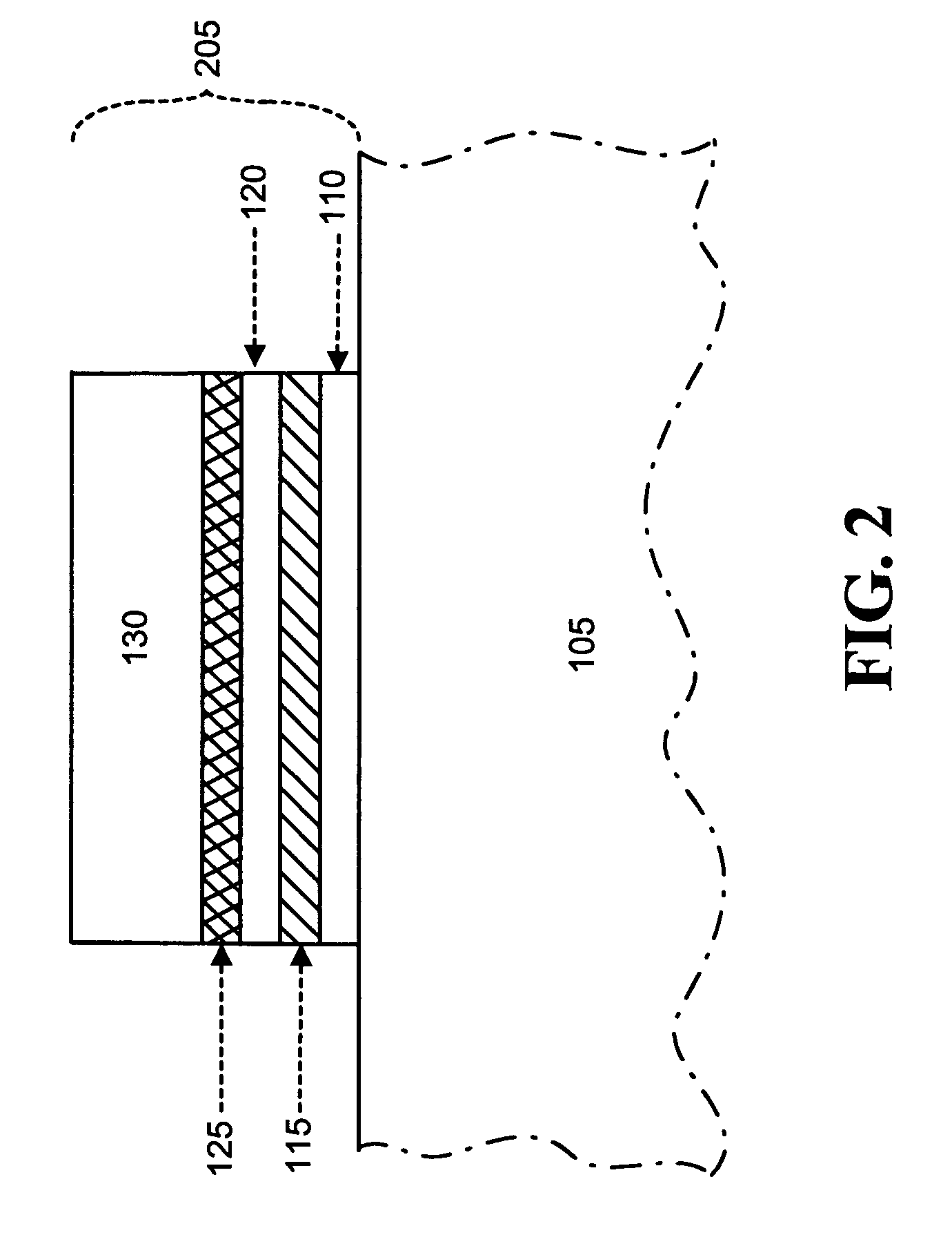
[0019]FIG. 1 illustrates a cross-section of a semiconductor substrate 105 according to an exemplary embodiment of the invention. Substrate 105, consistent with one aspect, may include a crystal silicon wafer. In other implementations, substrate 105 may include a gallium arsenide layer, a silicon-on-insulator structure, a germanium layer, a silicon-germanium layer, or other conventional materials used to form a semiconductor substrate. A bottom oxide layer 110 may be formed on substrate 105. Bottom oxide layer 110 may be formed on substrate 105 using, for example, existing deposition processes, such as a chemical vapor deposition (CVD) proc...


PUM


Abstract

A memory device may include a source region and a drain region formed in a substrate and a channel region formed in the substrate between the source and drain regions. The memory device may further include a first oxide layer formed over the channel region, the first oxide layer having a first dielectric constant, and a charge storage layer formed upon the first oxide layer. The memory device may further include a second oxide layer formed upon the charge storage layer, a layer of dielectric material formed upon the second oxide layer, the dielectric material having a second dielectric constant that is greater than the first dielectric constant, and a gate electrode formed upon the layer of dielectric material.

Description

TECHNICAL FIELD[0001]The present invention relates generally to semiconductor devices and, more particularly, to the use of a high dielectric constant (K) stack in a non-volatile memory semiconductor device.BACKGROUND ART[0002]Non-volatile memory devices are currently in widespread use in electronic components that require the retention of information when electrical power is terminated. Non-volatile memory devices include read-only-memory (ROM), programmable-read-only memory (PROM), erasable-programmable-read-only memory (EPROM), and electrically-erasable-programmable-read-only-memory (EEPROM) devices. EEPROM devices differ from other non-volatile memory devices in that they can be electrically programmed and erased. Flash EEPROM devices are similar to EEPROM devices in that memory cells can be programmed and erased electrically.[0003]Product development efforts in EEPROM device technology have focused on increasing the programming speed, lowering programming and reading voltages, ...

Claims


Application Information

Patent Timeline
Patent Type & Authority Patents(United States)
IPC IPC(8): H01L29/788H01L29/72
CPCH01L21/28282H01L29/792G11C16/0475H01L21/28273H01L29/40114H01L29/40117
Inventor ZHENG, WEIRANDOLPH, MARKSHIRAIWA, HIDEHIKO
Owner MONTEREY RES LLC
Why Eureka
Try Eureka