Complementary carbon nanotube triple gate technology

a carbon nanotube and triple gate technology, applied in the field of carbon nanotube field effect transistors, can solve the problem of difficult control of the threshold voltage (vt) of cntfets

Inactive Publication Date: 2009-02-17
GLOBALFOUNDRIES INC
View PDF27 Cites 47 Cited by
  • Summary
  • Abstract
  • Description
  • Claims
  • Application Information

AI Technical Summary

Benefits of technology

[0008]The second gates are positioned on the second side of the CNT opposite the source / drain electrodes. Specifically, second gates are positioned at each end of the CNT. As mentioned above, the second gates are adjusted to a preselected (either negative or positive) voltage in order to configure the CNTFET as either a p-FET or an n-FET, respectively. For example, a negative bias (i.e., a negative voltage) applied to the source / drain electrodes of the CNT(s) can promote the population of holes within the CNT, by pushing the Fermi level to the valence band and resulting in dominance of holes below the source / drain electrodes. The resulting structure acts as a p-FET. Alternatively, a positive bias (i.e., a positive voltage) applied to the source / drain electrodes of the CNT can promote the population of electrons within the CNT, by forcing the Fermi level to the conduction band and resulting in a dominance of electrons below the source / drain electrodes. The resulting structure acts as an n-FET. The second gates are formed such that there is a gap (i.e., a dielectric filled space) between the two second gates below the CNT. The gap between the two source / drain gates defines the area of the CNT that is not acted upon by the second gates and, thus, the size of this gap defines the channel region of the CNTFET. Additionally, the first and second gates can overlap to some degree (e.g., the first gate can be aligned above the gap and extend over a portion of the second gates) so as to optimize conduction in the carbon nanotube. Furthermore, the relative positioning of the first gate on the first side of the CNT and the second gates on the second side of the CNT minimizes parasitic capacitance between the second gates and the first gate and avoids parasitic resistance between the second gates and the source / drain electrodes.
[0009]Optionally, a third gate can be positioned on the second side of the CNT below the channel region. As mentioned above, the third gate can be biased to an additional preselected voltage to adjust the threshold voltage of the CNTFET. The third gate can be positioned closer to the CNT than the second gates to the extent that it does not obscure the effect of the second gates on the CNT in the vicinity of the source / drain electrodes. The third gate can also be positioned in the gap between the two second gates such that it is the same distance from the CNT as the second gates. However, the drive current of the CNTFET can be optimized by positioning the third gate below the gap such the gate dielectric of the third gate is thicker than that of both the first gate and the second gates. If the third gate is below the gap, then the size of the gap further defines the area of the carbon nanotube upon which the third gate can act (i.e., the area to which preselected potential can be imparted to adjust threshold voltage).

Problems solved by technology

However, there are two basic barriers to doing so.
Second, since the threshold voltage (Vt) of CNTFETs are not easily controlled via conventional means, such as doping of the channel, some means is required to adjust the threshold voltages to complementary CNTFETs-compatible values.

Method used


Image

  • Complementary carbon nanotube triple gate technology
  • Complementary carbon nanotube triple gate technology
  • Complementary carbon nanotube triple gate technology

Examples


Embodiment Construction

[0021]The embodiments of the invention and the various features and advantageous details thereof are explained more fully with reference to the non-limiting embodiments that are illustrated in the accompanying drawings and detailed in the following description. It should be noted that the features illustrated in the drawings are not necessarily drawn to scale. Descriptions of well-known components and processing techniques are omitted so as to not unnecessarily obscure the embodiments of the invention. The examples used herein are intended merely to facilitate an understanding of ways in which the embodiments of the invention may be practiced and to further enable those of skill in the art to practice the embodiments of the invention. Accordingly, the examples should not be construed as limiting the scope of the invention.

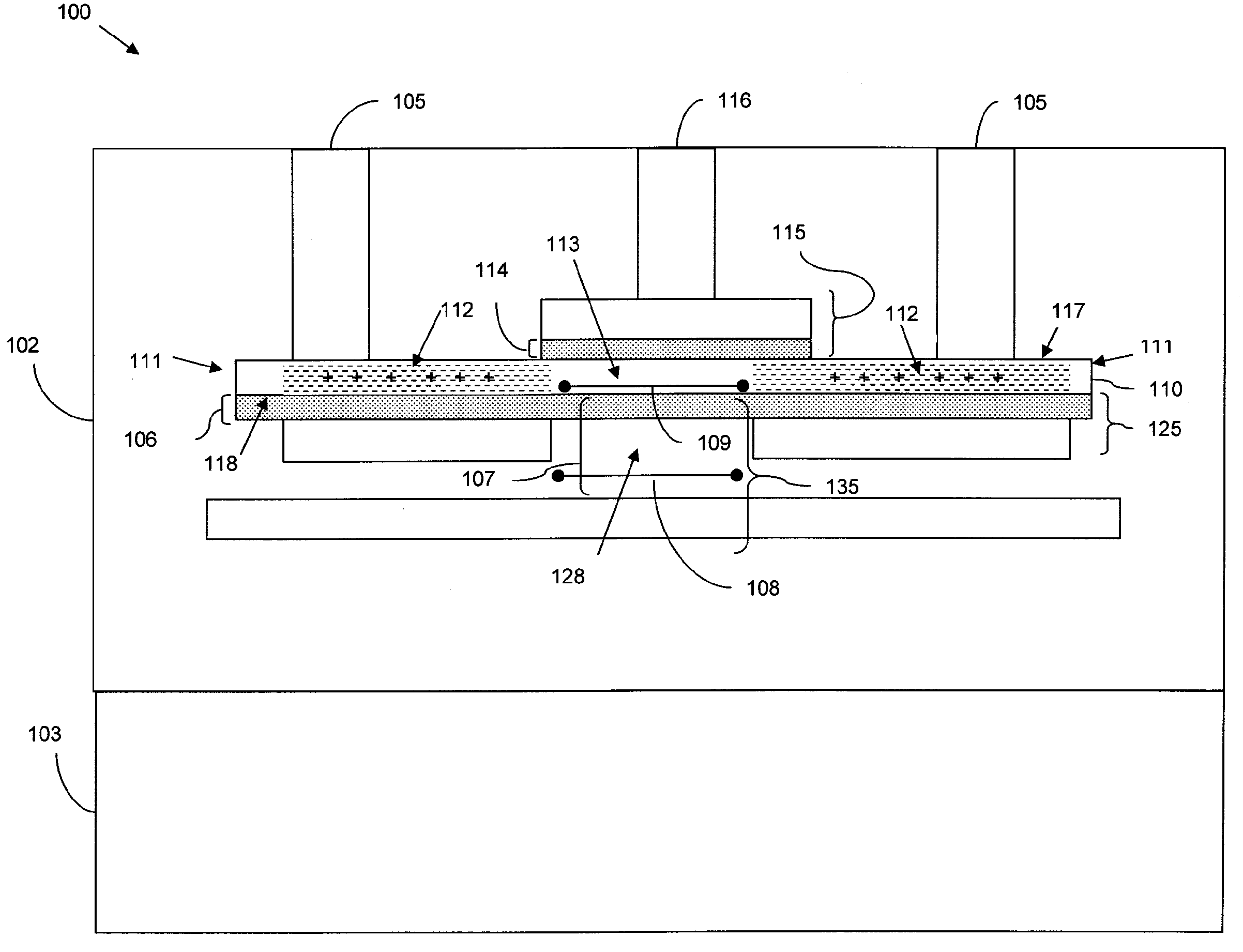
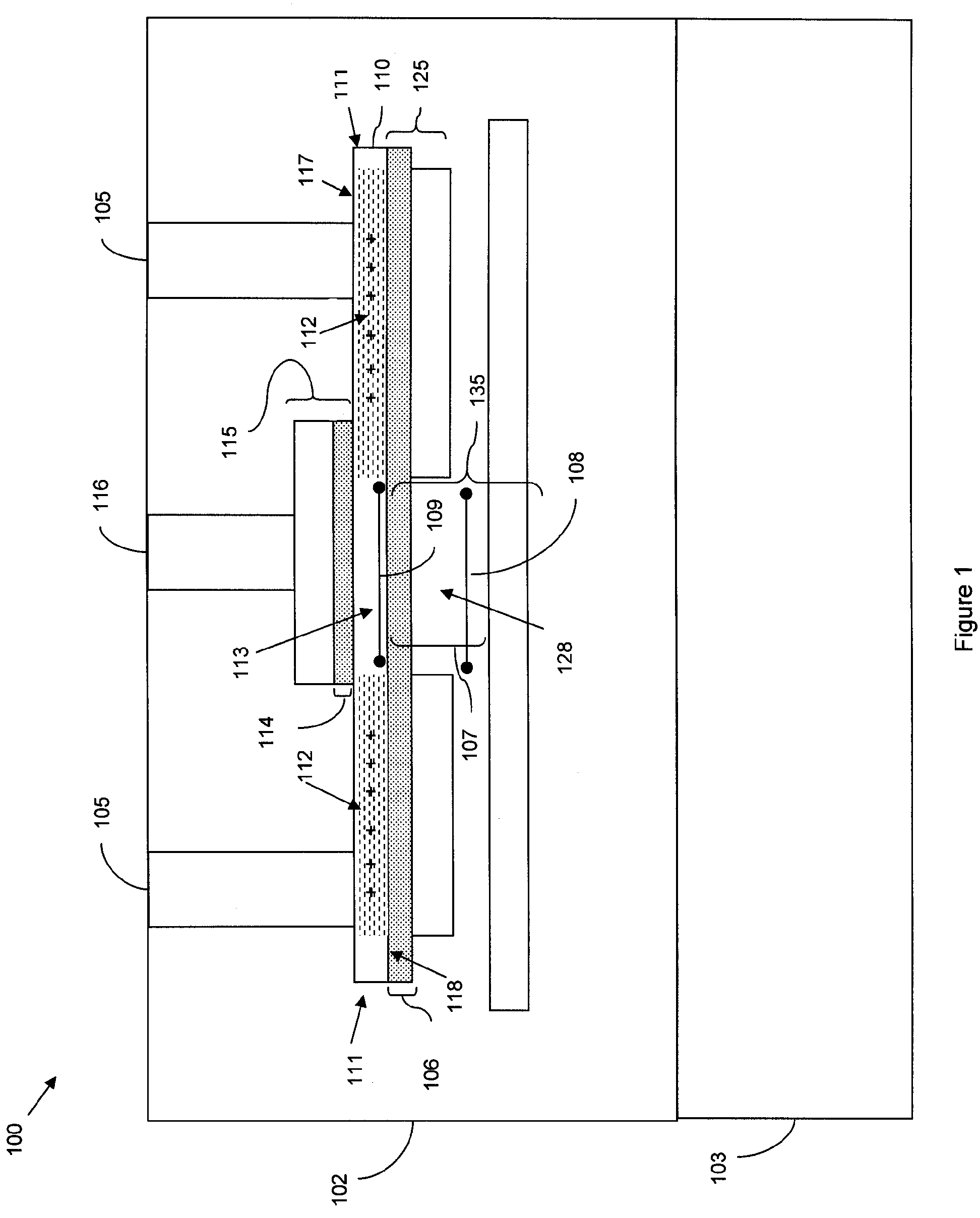
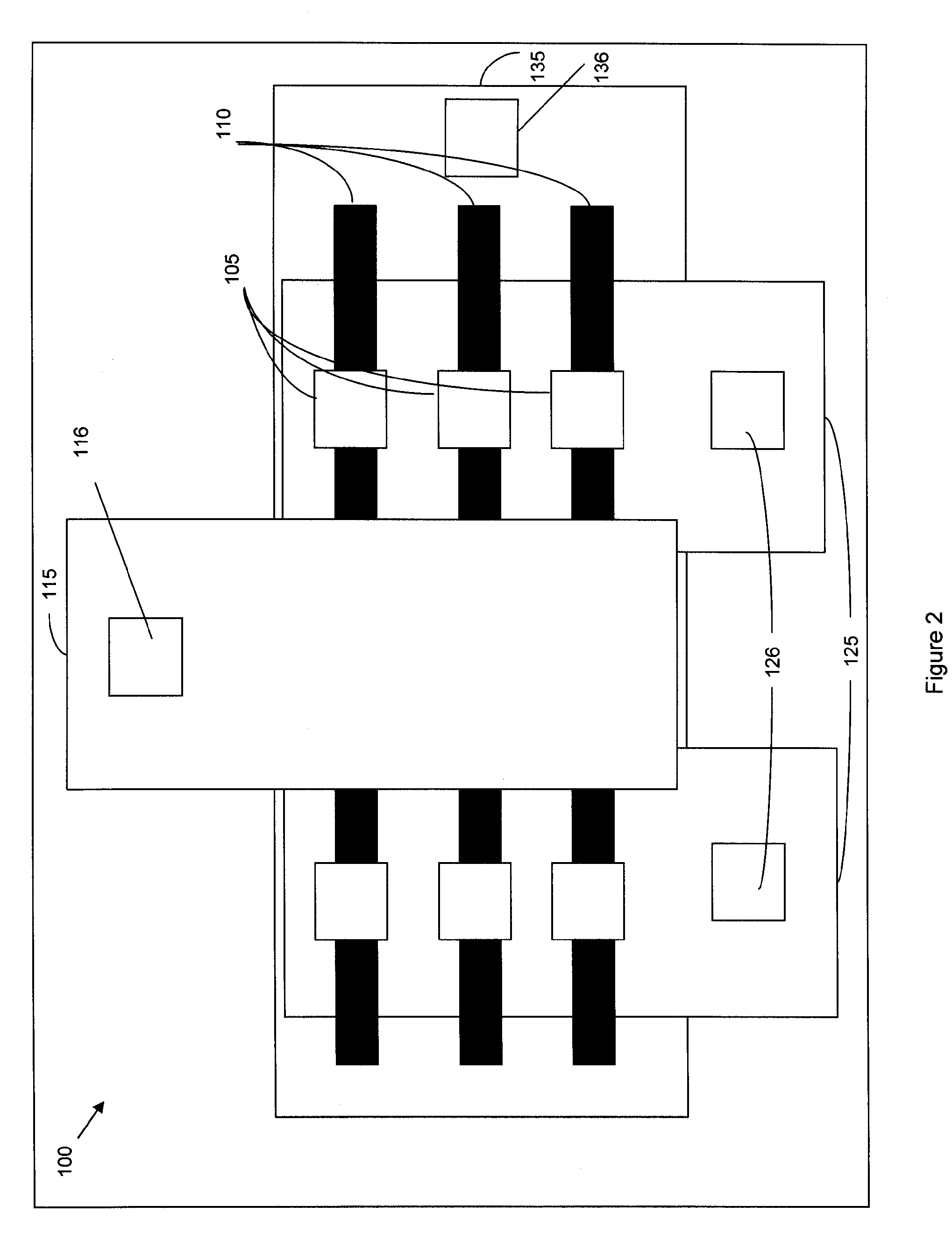
[0022]As mentioned above, the use of carbon nanotube (CNT) devices, such as CNT field effect transistors (CNTFETs), has been proposed to overcome scaling limits en...


PUM


Abstract

Disclosed is a CNT technology that overcomes the intrinsic ambipolar properties of CNTFETs. One embodiment of the invention provides either a stable p-type CNTFET or a stable n-type CNTFET. Another embodiment of the invention provides a complementary CNT device. In order to overcome the ambipolar properties of a CNTFET, source / drain gates are introduced below the CNT opposite the source / drain electrodes. These source / drain gates are used to apply either a positive or negative voltage to the ends of the CNT so as to configure the corresponding FET as either an n-type or p-type CNTFET, respectively. Two adjacent CNTFETs, configured such that one is an n-type CNTFET and the other is a p-type CNTFET, can be incorporated into a complementary CNT device. In order to independently adjust threshold voltage of an individual CNTFET, a back gate can also be introduced below the CNT and, particularly, below the channel region of the CNT opposite the front gate. In this manner parasitic capacitances and resistances are minimized.

Description

BACKGROUND OF THE INVENTION[0001]1. Field of the Invention[0002]The invention generally relates to carbon nanotube semiconductor devices, and, more particularly, to a carbon nanotube field effect transistor that is configured to overcome intrinsic ambipolar properties and to allow for threshold voltage adjustments and to complementary carbon nanotube devices that incorporate such transistors.[0003]2. Description of the Related Art[0004]A carbon nanotube (i.e., nanoscale hollow graphite tube) can, depending on its conformational geometry, exhibit either metallic or semiconductor properties. In recent years the use of semiconductor carbon nanotube (CNT) devices, such as CNT field effect transistors (CNTFETs), has been proposed to overcome scaling limits encountered by silicon semiconductor devices. Additionally, since semiconductor CNTs exhibit high transconductance, a desirable property for complementary devices, such as complementary inverters, complementary CNTFET circuitry which m...

Claims


Application Information

Patent Timeline
Patent Type & Authority Patents(United States)
IPC IPC(8): H01L27/092
CPCB82Y10/00H01L27/283H01L51/055H01L51/0048H01L51/0558Y10S977/742Y10S977/94H10K19/10H10K85/221H10K10/481H10K10/484
Inventor CHEN, JIANOWAK, EDWARD J.
Owner GLOBALFOUNDRIES INC
Why Eureka
Try Eureka