Systems and methods for forming multiple fin structures using metal-induced-crystallization

a technology of metal crystallization and multiple fins, applied in the field of semiconductor devices, can solve the problems of difficult, if not impossible, scaling of existing bulk mosfet devices below the 0.1 m process generation, and achieve the effect of small pitch

Inactive Publication Date: 2009-03-03
ALSEPHINA INNOVATIONS INC
View PDF42 Cites 8 Cited by
  • Summary
  • Abstract
  • Description
  • Claims
  • Application Information

AI Technical Summary

Benefits of technology

[0005]Implementations consistent with the principles of the invention provide multiple silicon fin structures formed on a semicondu...

Problems solved by technology

Due to limitations associated with gate-oxide thicknesses and source/drain (S/D) junction depths, scal...

Method used


Image

  • Systems and methods for forming multiple fin structures using metal-induced-crystallization
  • Systems and methods for forming multiple fin structures using metal-induced-crystallization
  • Systems and methods for forming multiple fin structures using metal-induced-crystallization

Examples


Embodiment Construction

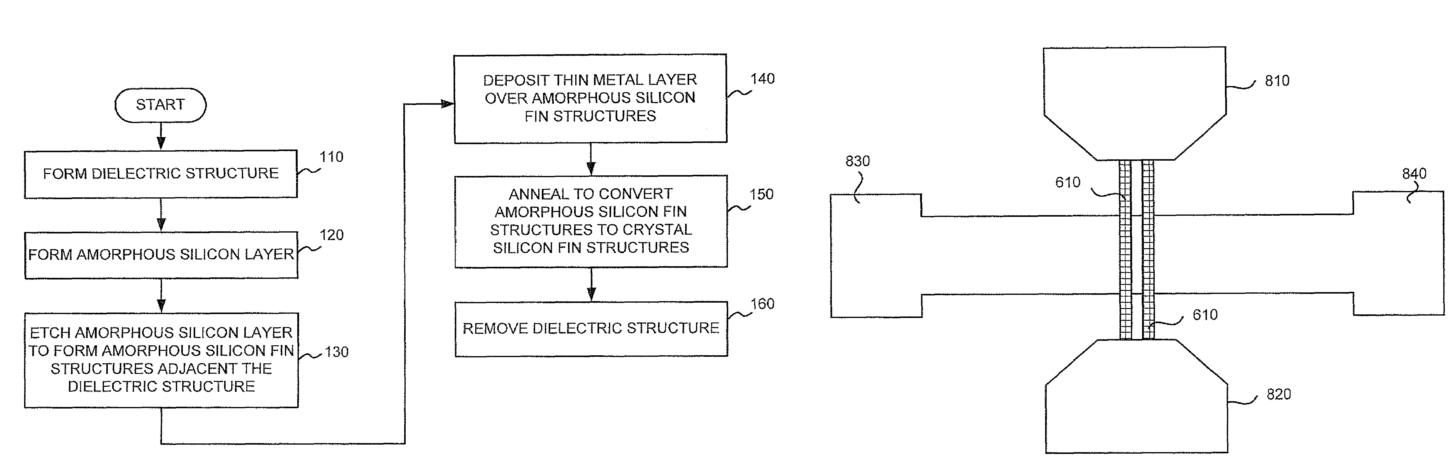
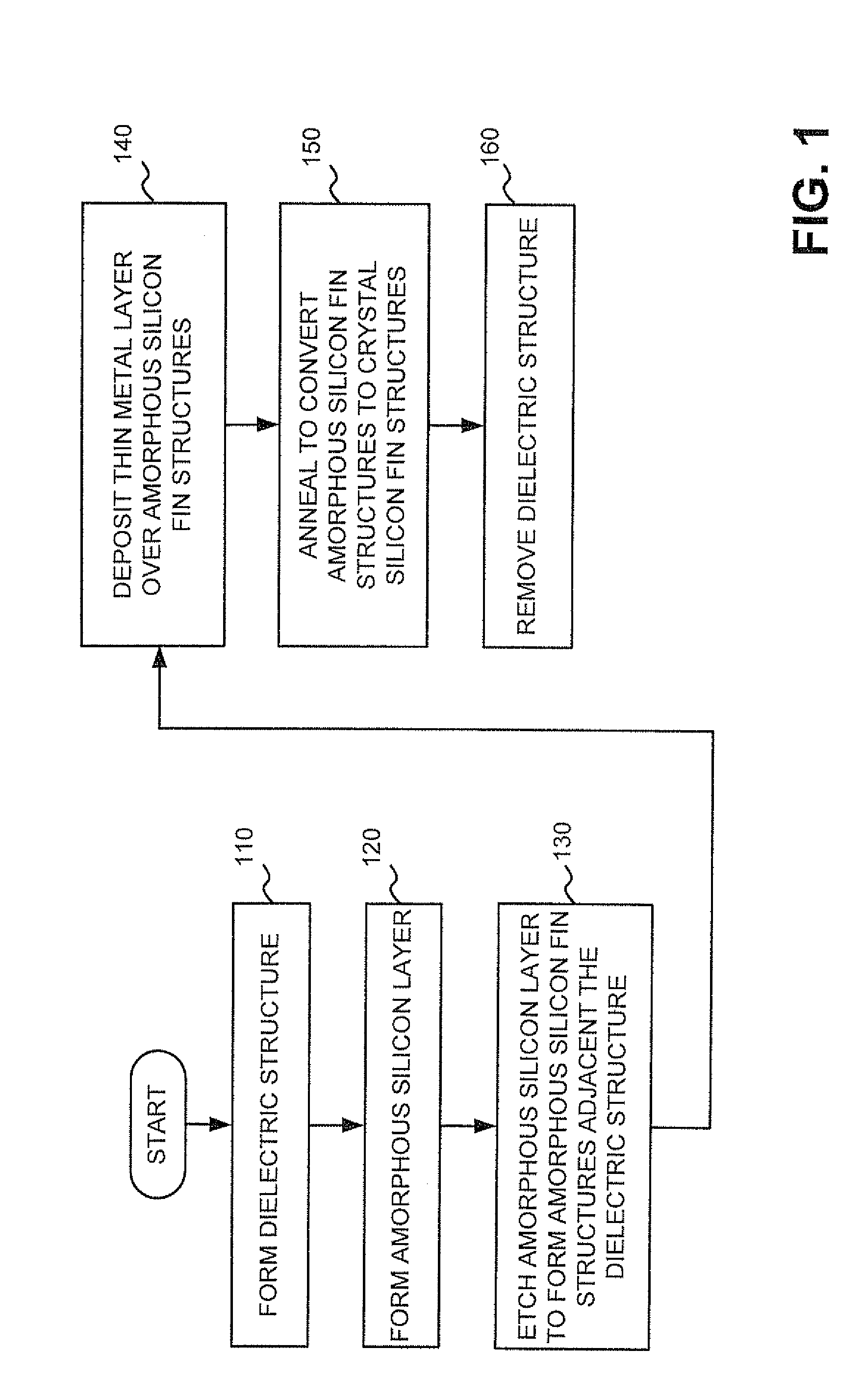
[0014]The following detailed description of implementations consistent with the present invention refers to the accompanying drawings. The same reference numbers in different drawings may identify the same or similar elements. Also, the following detailed description does not limit the invention. Instead, the scope of the invention is defined by the appended claims and their equivalents.

[0015]Implementations consistent with the principles of the invention provide crystalline silicon fin structures that are formed on a semiconductor device. FinFET channel width is defined by the height of the fin. The fin height is typically limited due to patterning concerns, affecting the drive current. Implementations consistent with the principles of the invention use multiple fin structures in order to achieve the desired drive current. For area efficiency, the multiple fin structures may be densely provided (i.e., formed in close proximity to each other).

Exemplary Processing

[0016]FIG. 1 illustr...


PUM


Abstract

A method for forming fin structures for a semiconductor device that includes a substrate and a dielectric layer formed on the substrate is provided. The method includes etching the dielectric layer to form a first structure, depositing an amorphous silicon layer over the first structure, and etching the amorphous silicon layer to form second and third fin structures adjacent first and second side surfaces of the first structure. The second and third fin structures may include amorphous silicon material. The method further includes depositing a metal layer on upper surfaces of the second and third fin structures, performing a metal-induced crystallization operation to convert the amorphous silicon material of the second and third fin structures to a crystalline silicon material, and removing the first structure.

Description

RELATED APPLICATION[0001]This application is a divisional of U.S. patent application Ser. No. 10 / 726,569, filed Dec. 4, 2003, the disclosure of which is incorporated by reference herein.FIELD OF THE INVENTION[0002]The present invention relates generally to semiconductor manufacturing and, more particularly, to FinFET devices that include multiple silicon fin structures and a method for forming the fin structures.BACKGROUND OF THE INVENTION[0003]Scaling of device dimensions has been a primary factor driving improvements in integrated circuit performance and reduction in integrated circuit cost. Due to limitations associated with gate-oxide thicknesses and source / drain (S / D) junction depths, scaling of existing bulk MOSFET devices below the 0.1 μm process generation may be difficult, if not impossible. New device structures and new materials, thus, are likely to be needed to improve FET performance.[0004]Double-gate MOSFETs represent devices that are candidates for succeeding existing...

Claims


Application Information

Patent Timeline
IPC IPC(8): H01L21/336H01L21/3205H01L21/4763
CPCH01L29/66795H01L21/02532H01L21/02672H01L29/785
Inventor WANG, HAIHONGAHMED, SHIBLY S.LIN, MING-RENYU, BIN
Owner ALSEPHINA INNOVATIONS INC
Why Eureka
Try Eureka