
Skew-reducing signal line sub-driver circuits, methods and systems

a technology of driver circuit and signal line, applied in the field of digital signal line driver circuit, methods and systems, can solve the problems of limiting the ultimate speed of the circuit, skew between/between adjacent signal lines may become increasingly problematic, and skew may become more problematic, so as to reduce skew

Active Publication Date: 2009-03-03
SAMSUNG ELECTRONICS CO LTD
View PDF5 Cites 0 Cited by
  • Summary
  • Abstract
  • Description
  • Claims
  • Application Information

AI Technical Summary

Benefits of technology

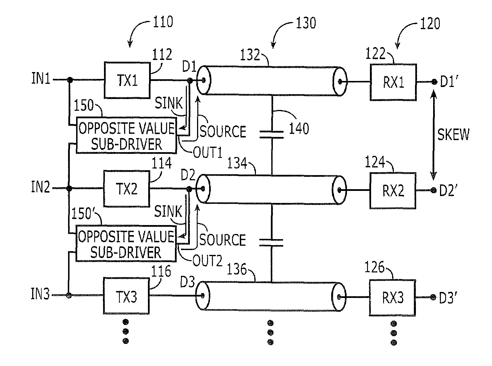
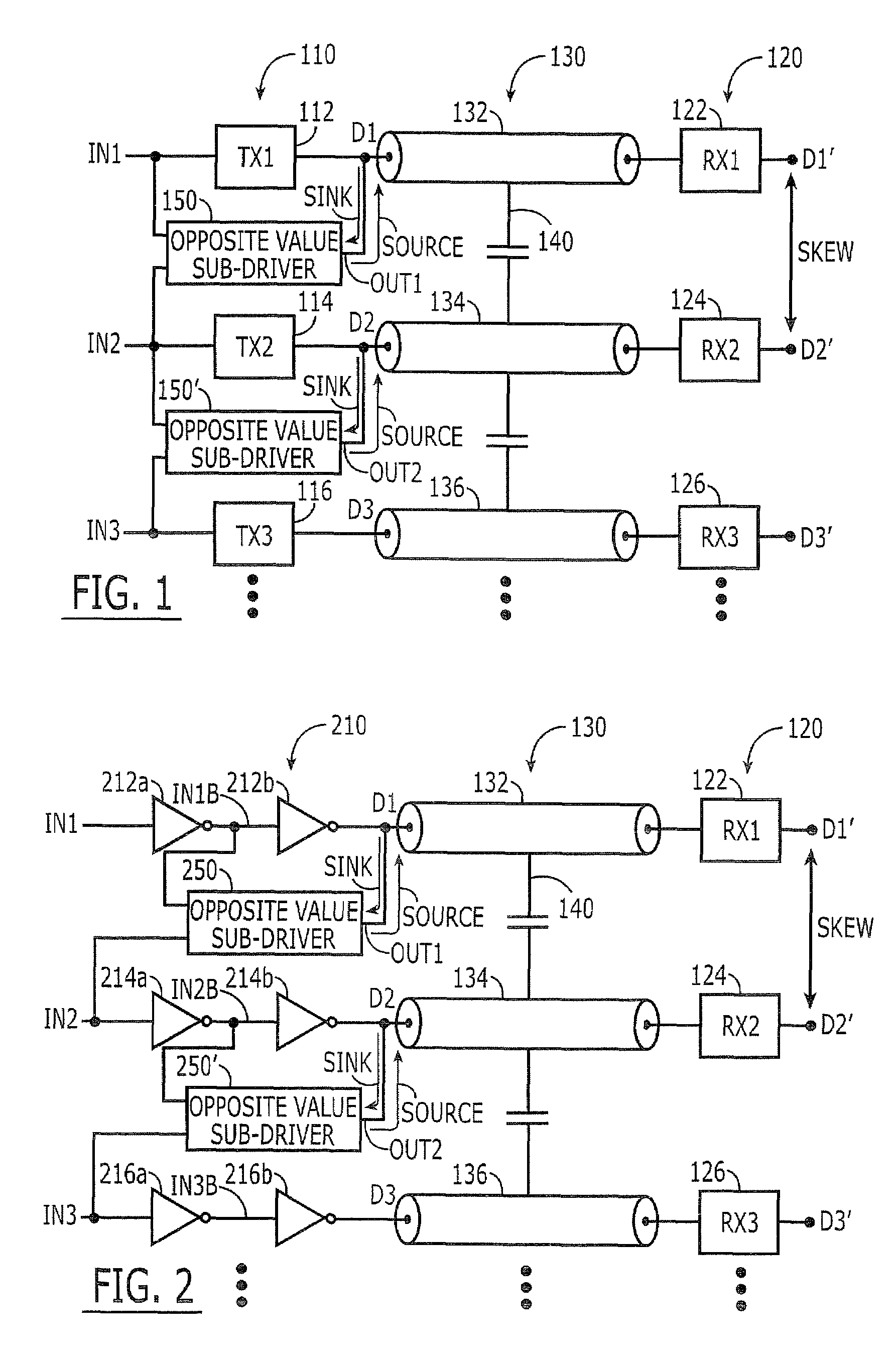
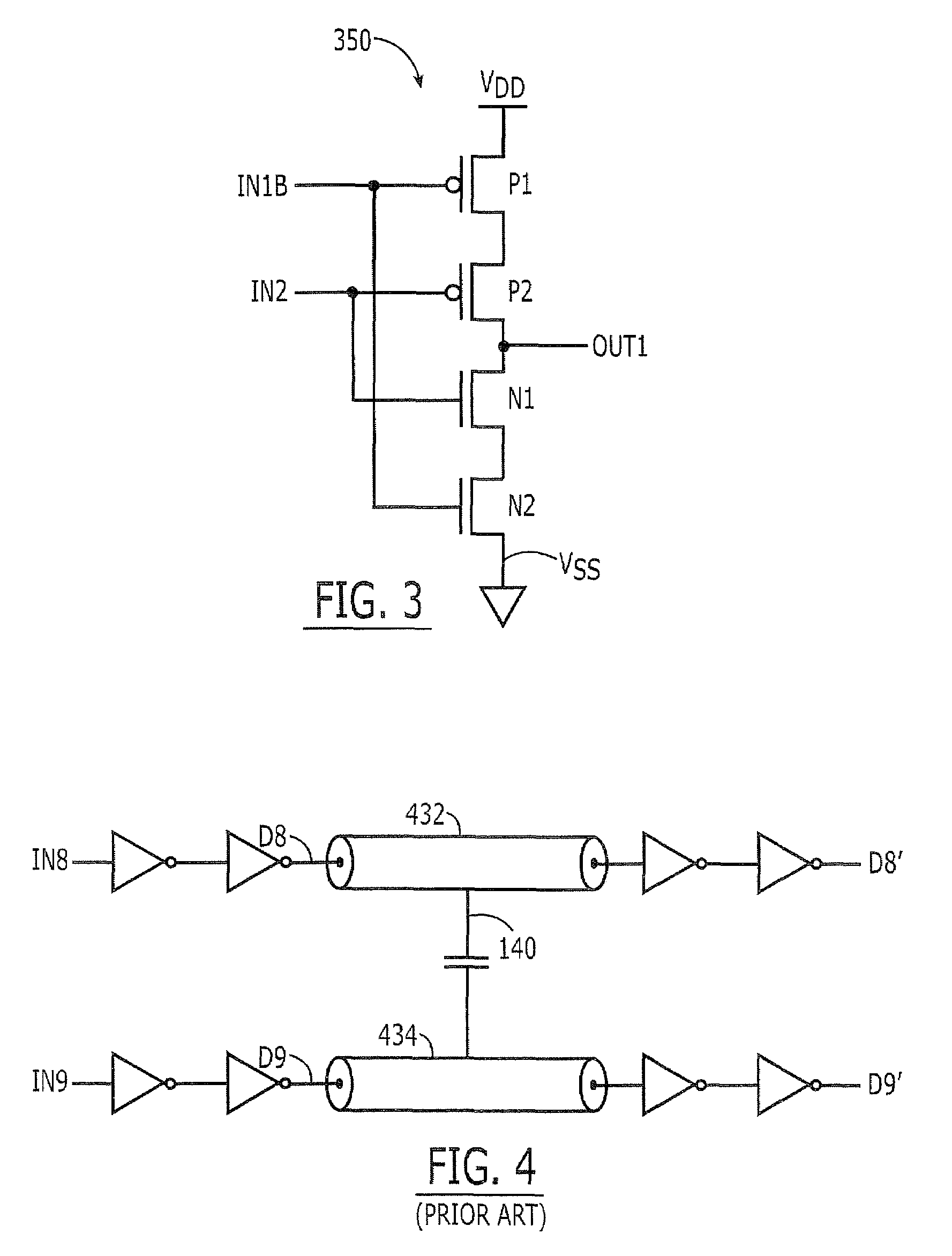
The present invention provides circuits and methods for reducing skew between digital signals transmitted over signal lines. This is achieved by using sub-drivers that source or sink current to or from the signal lines based on the input of the digital signals. The sub-drivers may be controlled by a controlling electrode and may be connected to a power supply or ground voltage. The methods may involve sourcing or sinking additional current to or from the signal lines to achieve the desired reduction in skew. The technical effect of this invention is to improve the timing accuracy and reliability of digital signal transmission in electronic circuits.

Problems solved by technology

As the clock speeds of digital signals continue to increase, for example approaching 1 GHz or more, skew between / among adjacent signal lines may become increasingly problematic.
As is well known to those having skill in the art, there are many potential causes of skew.
This line length difference may cause skew.
Moreover, the different signal lines may have different capacitances (actual and / or parasitic), which may also cause skew.
The signals being transmitted over different signal lines may also pass through different numbers of gates, which may also cause skew.
Skew also may be caused when output drivers have different output impedance and / or when different types of gates are used.
There may also be other causes of skew.
As the transmission speeds of digital signals continue to increase, skew may become more problematic.
In particular, skew may limit the ultimate speed of the circuit and / or may reduce the operating margins thereof.
Unfortunately, this may increase the complexity of the transmitting or receiving circuit, and may also be difficult to implement when the time delay difference is variable.
Unfortunately, these techniques may also add to the circuit complexity and a DLL / PLL may introduce its own delay due to locking time of the DLL / PLL.

Method used


Image

  • Skew-reducing signal line sub-driver circuits, methods and systems
  • Skew-reducing signal line sub-driver circuits, methods and systems
  • Skew-reducing signal line sub-driver circuits, methods and systems

Examples


case2

[0043]Case2 illustrates both the first and second input signals simultaneously undergoing a same transition in logical value (shown as from logic low to logic high in Case2). As shown in Case2, D1′ and D2′ are delayed by the same amount that D8′ is delayed, so that the amount of delay indicated by “Gap 1”, “Gap 2” and “Gap 3” is the same. Again, as was the case in Case1, sub-driver circuits and methods according to some embodiments of the invention do not effect the delay time.

[0044]In contrast, in Case3, the first and second digital signals undergo opposite simultaneous transitions, with IN1 transitioning from logic low to logic high and IN2 transitioning from logic high to logic low. As shown for Case3, D1′ and D2′ have reduced skew, as shown by “Gap 4” and “Gap 5”, compared to skew created on D9′, as indicated by “Gap 6”. Accordingly, sub-driver circuits and methods according to embodiments of the present invention can reduce skew for simultaneous opposite value transitions compa...


PUM


Abstract

Circuits, methods and systems are provided to reduce skew between a first digital signal that is transmitted by a first driver circuit over a first signal line, and a second digital signal that is transmitted by a second driver circuit over a second signal line. Skew may be reduced by sourcing or sinking additional current to or from the first signal line in response to the first digital signal and the second digital signal transitioning to opposite logical values, and otherwise refraining from sourcing or sinking the additional current to or from the first signal line. Skew may also be reduced between the first digital signal that is transmitted by the first driver circuit over the first signal line and a third digital signal that is transmitted by a third driver circuit over a third signal line by sourcing or sinking additional current to or from the first signal line in response to the first digital signal and the third digital signal transitioning to opposite logical values, and to otherwise refrain from sourcing or sinking the additional current to or from the first signal line.

Description

FIELD OF THE INVENTION[0001]This invention relates to digital signal line drivers, methods and systems, and more particularly to skew-reducing digital signal line driver circuits, methods and systems.BACKGROUND OF THE INVENTION[0002]Digital signal lines are used to transmit digital signals between a transmitter and a receiver. The signal lines may be “on-chipsignal lines that connect various subsystems on a single integrated circuit chip. For example, on-chip signal lines may connect a memory subsystem with a processor or host subsystem on a single integrated circuit chip. The on-chip digital signals may be, for example, data signals from a memory subsystem, often referred to as “DQ” signals. Alternatively, the signal lines may be “off-chip” signal lines, wherein output drivers drive a digital signal off an integrated circuit chip over a signal line that connects a given chip with another chip, another level of packaging or with an external system.[0003]As the clock speeds of digi...

Claims


Application Information

Patent Timeline
Patent Type & Authority Patents(United States)
IPC IPC(8): H03K3/00
CPCH04L25/0264H04B3/04
Inventor JANG, SEONG-JIN
Owner SAMSUNG ELECTRONICS CO LTD
Learn More