Driving circuit that eliminates effects of ambient temperature variations and increases driving capacity

a driving circuit and ambient temperature technology, applied in the direction of logic circuit coupling/interface arrangement, pulse manipulation, pulse technique, etc., can solve the problems of increasing the difficulty of developing an operable lsi, increasing the difficulty of operating timing, so as to increase the driving capacity and prevent or reduce the current through the transistor

Active Publication Date: 2009-03-24
LAPIS SEMICON CO LTD
View PDF5 Cites 29 Cited by
  • Summary
  • Abstract
  • Description
  • Claims
  • Application Information

AI Technical Summary

Benefits of technology

[0010]An object of the invention is to eliminate the effect of the ambient temperature variations.
[0025]When the input signal changes (e.g., rises), the output node is driven by the driving section, as well as by the transistor connected between the predetermined potential node, (e.g., the power supply potential node) and the output node. As a result, even when the ambient temperature rises and the delay time of the driving section is increased, because of the additional driving by means of the transistor, the variation in the delay time due to the temperature change can be restrained.
[0039]By the provision of the transistor connected between the output node and the predetermined potential node (e.g., the power supply potential node), the driving capacity can be increased, and yet the through current through the transistor can be prevented or reduced.

Problems solved by technology

The conventional driving circuit having CMOS inverters has the following problems.(A1) The delay time at each part of the circuit varies with the ambient temperature, causing irregularities with respect to operation timings.
However, because of the increase in the size of the LSI, and the miniaturization of each element in the circuit, the variations continue to increase, so that it is becoming more and more difficult to develop an operable LSI unless the variations are restrained.
Such a through current causes waste of power.
The through current leads to increase in the consumption current in the LSI as a whole.
To cope with the temperature increase, an expensive package may have to be used, resulting in increase in the cost of the product.
Moreover, the increased consumption current may be an obstacle in applications to portable equipment.(A3) Parts of the LSI found to be affected by cross-talk after the layout design need to be modified by changing the wiring of the conductors, and / or changing the position of the driving circuits, to avoid cross-talk.
However, such a modification may be difficult depending on the initial layout, and substantial revision of the circuit design or the layout design may be required.(A4) The driving capacity of the driving section, such as CMOS inverters may not be sufficient for certain applications.

Method used


Image

  • Driving circuit that eliminates effects of ambient temperature variations and increases driving capacity
  • Driving circuit that eliminates effects of ambient temperature variations and increases driving capacity
  • Driving circuit that eliminates effects of ambient temperature variations and increases driving capacity

Examples


embodiment 1

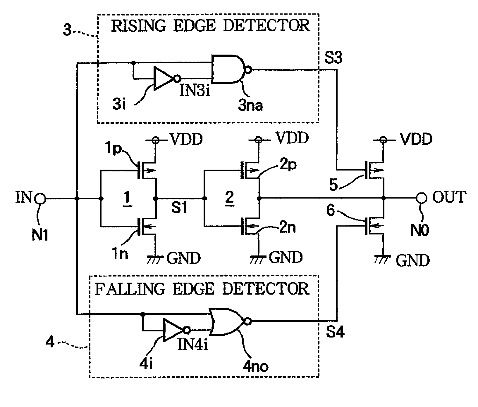
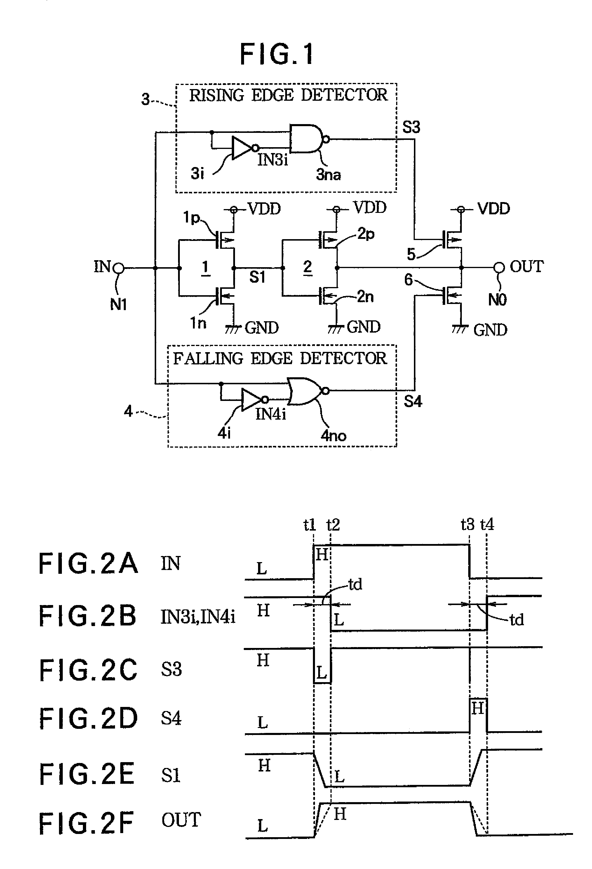
[0045]FIG. 1 shows a driving circuit of Embodiment 1 of the present invention.

[0046]The illustrated circuit includes an input node NI at which an input signal IN is supplied. Connected to the input node NI is a first CMOS inverter 1 comprising a PMOS 1p and an NMOS in connected between a power supply potential node VDD and a ground potential node GND.

[0047]Connected to the output side of the CMOS inverter 1 is a second CMOS inverter 2 comprising a PMOS 2p and an NMOS 2n connected between the power supply potential node VDD and the ground potential node GND. The output side of this CMOS inverter 2 is connected to an output node NO, through which the output signal OUT is output. Connected to the input node NI of the driving circuit is a rising edge detector 3 and a falling edge detector 4. The first and the second CMOS inverters 1 and 2 in combination form a driving section for power-amplifying the input signal, and outputting an amplified signal to the output node NO.

[0048]A PMOS 5 i...

embodiment 2

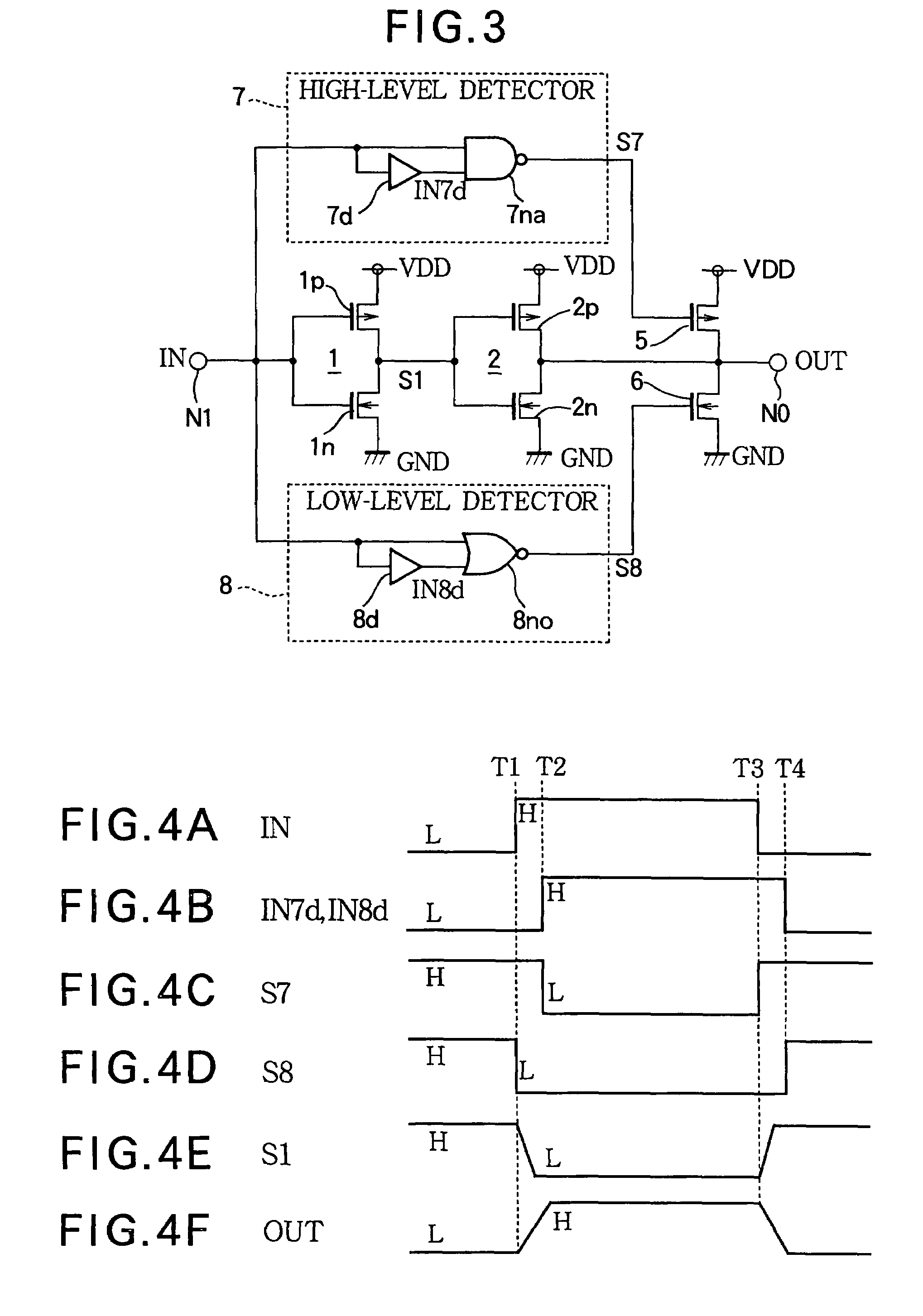
[0065]FIG. 3 shows a driving circuit according Embodiment 2 of the present invention. Reference numerals identical to those in FIG. 1 denote identical or corresponding elements.

[0066]The driving circuit shown in FIG. 3 is provided with a high-level detector 7, serving as a first detector in place of the rising edge detector 3, and a low-level detector 8, serving as a second detector, in place of the falling edge detector 4.

[0067]The high-level detector 7 outputs a high-level detection signal S7 which goes “L” upon expiration of a certain time period after the input signal IN rises from “L” to “H”. When the input signal IN falls from “H” to “L”, the high-level detection signal S7 is returned to “H” instantly. The falling and rising of the high-level detection signal S7 may be described as “commencement” and “termination” of the high-level detection signal S7. The high-level detector 7 comprises a delay element 7d for delaying the input signal IN by a certain time period, and a NAND g...


PUM


Abstract

In addition to two-stage CMOS inverters inverting and amplifying the input signal, a rising edge detector detects the rising edge of the input signal, and outputs a rising edge detection signal having a pulse width corresponding to ambient temperature, a PMOS drives the output node to the power supply potential according to the rising edge detection signal, a falling edge detector detects the falling edge of the input signal and outputs a falling edge detection signal having a pulse width corresponding to ambient temperature, and an NMOS drives the output node to ground potential according to the falling edge detection signal. When ambient temperature rises, and delay time of the inverters are thereby increased, pulse widths of the rising and falling edge detection signals are increased. The additional driving restrains delay time variation in a driving circuit due to ambient temperature change.

Description

BACKGROUND OF THE INVENTION[0001]1. Field of the Invention[0002]The present invention relates a driving circuit (driver) provided in an output stage of an LSI (large-scale integrated circuit) for driving a circuit connected externally to the LSI.[0003]2. Description of the Background Art[0004]A conventional circuit provided in an output stage of an LSI to drive a circuit connected to and provided externally to the LSI, comprises a plurality of stages of CMOS inverters, as described for example in Japanese Patent Kokai Publication No. 2003-133943.[0005]The conventional driving circuit having CMOS inverters has the following problems.[0006](A1) The delay time at each part of the circuit varies with the ambient temperature, causing irregularities with respect to operation timings. In designing an LSI, it was therefore necessary to allow for the variations in the operation timings. However, because of the increase in the size of the LSI, and the miniaturization of each element in the ci...

Claims


Application Information

Patent Timeline
Patent Type & Authority Patents(United States)
IPC IPC(8): H03K3/00
CPCH03K5/1534H03K17/122H03K17/145H03K17/162H03K17/6872H03K19/00384H03K19/01707H03K17/04106
Inventor TOKUNO, YOSHIO
Owner LAPIS SEMICON CO LTD
Why Eureka
Try Eureka