Method of making an electronic assembly

a technology of electronic assembly and assembly body, which is applied in the direction of manufacturing tools, electrical apparatus contruction details, and soldering apparatus, etc., can solve the problems of process yield loss and vulnerable electronic components, and achieve the effects of reducing yield loss, improving long-term reliability of solder joints, and retaining strength

Inactive Publication Date: 2009-03-31
APPLE INC
View PDF7 Cites 18 Cited by
  • Summary
  • Abstract
  • Description
  • Claims
  • Application Information

AI Technical Summary

Benefits of technology

[0008]This invention provides a method of making an electronic assembly having an electric component that is underfilled in a unique manner to reduce yield loss. The underfill method improves long-term reliability of the solder joint between the electronic component and the circuit board of the electronic assembly. The underfill method preferably uses an epoxy material that compliments the solder bumps and retains their strength for years.

Problems solved by technology

The electronic component is vulnerable to damage due to handling and electrical testing.
This process has an appreciable yield loss due to underfill accidentally curing on the top of the electronic device which interferes with heat transfer when a heat sink is used.

Method used


Image

  • Method of making an electronic assembly
  • Method of making an electronic assembly
  • Method of making an electronic assembly

Examples


Embodiment Construction

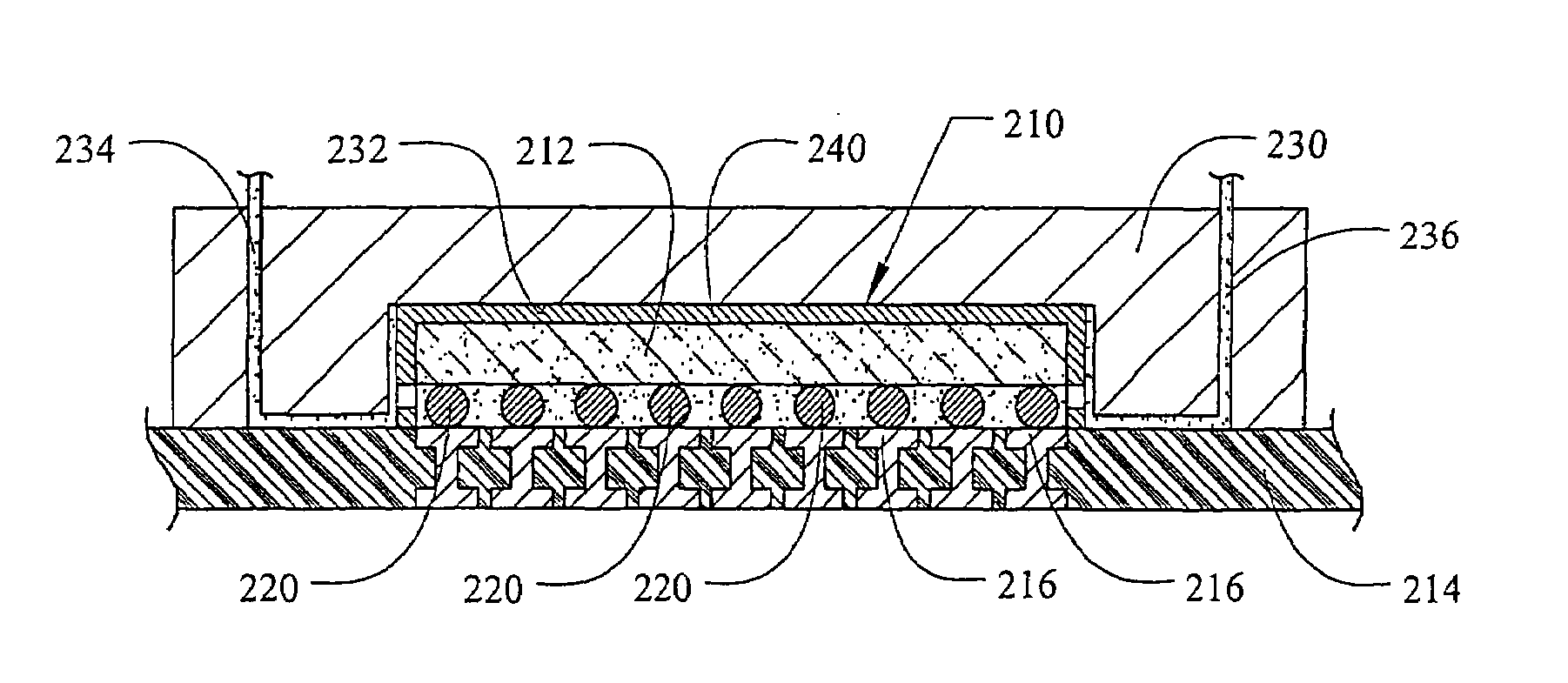
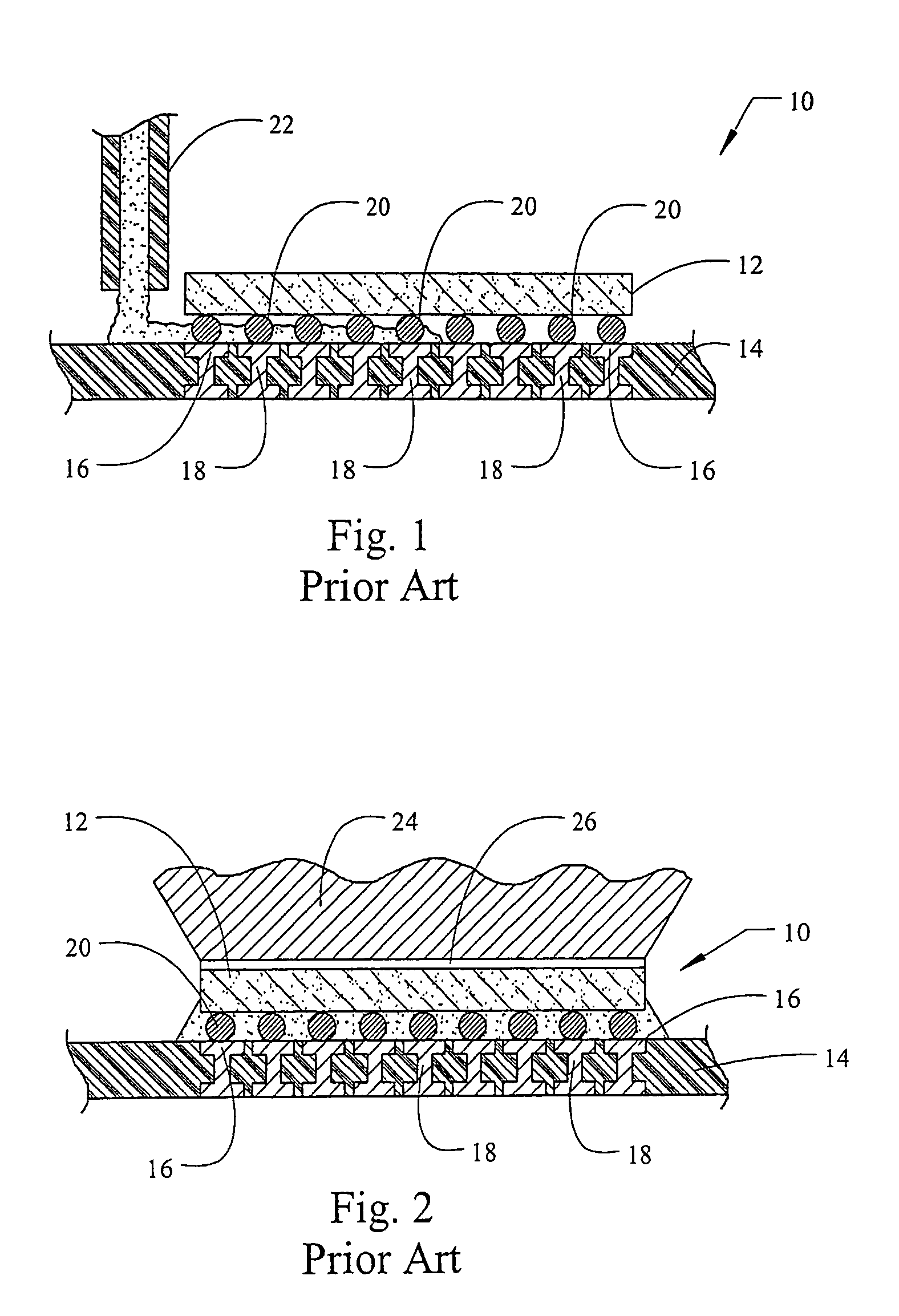
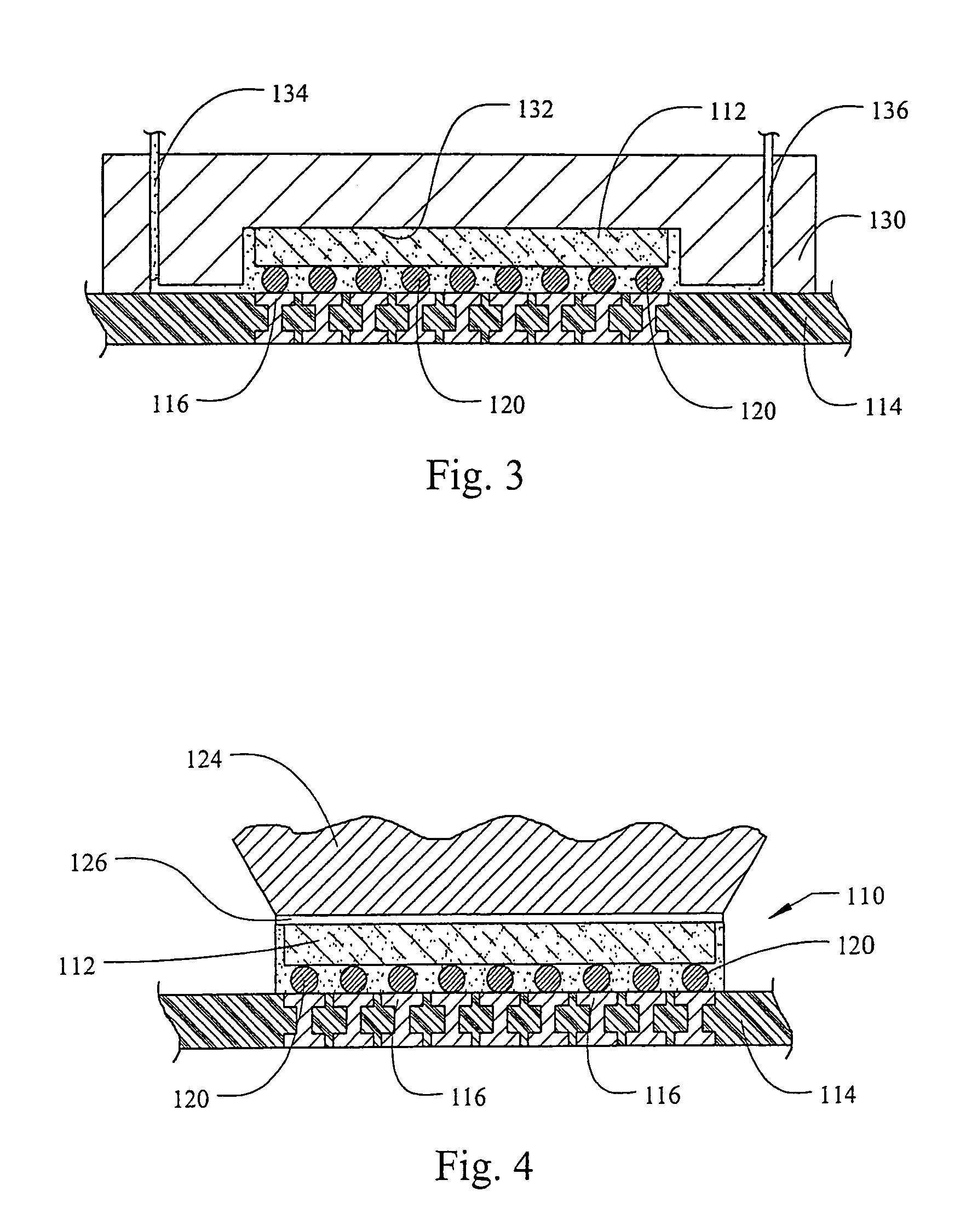
[0017]FIGS. 1 and 2 illustrate a prior art method of making an electronic assembly 10 comprising an electronic component 12, such as a flip chip, and a circuit board 14. The prior art and the invention methods are described in connection with one electronic component being attached to a circuit board. However, circuit boards typically have several electronic components of various sizes and complexities attached to them, some or all of which may be attached to the circuit board utilizing the method of the invention.

[0018]The typical circuit board 14 is basically a substrate of insulation material that carries traces of electrically conductive material such as copper, forming electrical circuits that include contact pads for making electrical connections. Electrical and electronic components are attached to the circuit board and connected electrically to the electrical circuits using contact pads on the top surface of the circuit board. In many instances the circuit board is a laminat...


PUM

PropertyMeasurementUnit
temperatureaaaaaaaaaa
pressureaaaaaaaaaa

Abstract

A method of making an electronic assembly comprising an electronic component that is attached to a circuit board by protruding solder bumps of the electronic component places the electronic component on a surface of the circuit board so that solder bumps on the bottom of the electronic component engage contact pads on the top of the circuit board. The solder bumps are then reflowed to attach the electronic component to the circuit board after which the electronic component is underfilled by providing a mold die having a mold cavity, a gate leading into the mold cavity and a vent leading out of the mold cavity. The mold die is placed over the electronic component and onto the surface of the circuit board so that the electronic component is inside the mold cavity and the mold cavity is sealed. An encapsulating material, preferably an epoxy material, is transferred or injected into the mold cavity to fill space between the respective surfaces of the electronic component and the circuit board and then cured to encapsulate the solder bumps that have been reflowed. An optional integrated heat sink for the electronic component may be used when practicing the method of the invention to make an electronic assembly.

Description

FIELD OF THE INVENTION[0001]This invention relates to a method of making an electronic assembly.BACKGROUND OF THE INVENTION[0002]A typical electronic assembly is circuit board that has electronic components, such as PBGAs and flip chips, attached to it. Each of these electronic components has solder bumps on the bottom that are reflowed to attach the electronic component to contact pads on the circuit board.[0003]Consequently, it is conventional practice to underfill the electronic component with a polymeric material after it is attached to the circuit board. The electronic component is vulnerable to damage due to handling and electrical testing. The bottom of the electronic component must be cleaned of flux residue in order for epoxy underfill to be used.[0004]In the present underfill process a liquid polymeric material is dispensed through a needle to two sides of the attached electronic component and then the needle progresses to another attached electronic component to repeat th...

Claims


Application Information

Patent Timeline
Patent Type & Authority Patents(United States)
IPC IPC(8): H01L23/48B23K31/02
CPCH01L21/563H01L21/565H01L24/28H01L2224/73253H01L2224/73204H01L2224/32225H01L2924/14H01L2924/01082H01L2924/01029H01L2224/92125H01L2224/83102H01L2224/16225H01L2224/73203H01L2924/00
Inventor LAWLYES, DANIEL A.LAUDICK, DAVID A.
Owner APPLE INC
Why Eureka
Try Eureka