Semiconductor integrated circuit for high-speed, high-frequency signal transmission

a high-speed, high-frequency signal technology, applied in the direction of transistors, instruments, static storage, etc., can solve the problems of increasing the capacitance of a depletion layer, and requiring time to change the material, etc., to achieve fast switching, high-speed operation, and faster operation

Active Publication Date: 2009-03-31
LONGITUDE LICENSING LTD
View PDF4 Cites 9 Cited by
  • Summary
  • Abstract
  • Description
  • Claims
  • Application Information

AI Technical Summary

Benefits of technology

[0009]It is an object of the present invention to provide a semiconductor integrated circuit enabling fast switching operation while avoiding much time taken in the state transition caused by an increase in a capacitance when high-speed differential signals are supplied to a MOS transistor.
[0011]According to the aspect of the invention, in driving a pair of MOS transistors (pair transistors) with high-speed signals, fast charge supply is required corresponding to the capacitance of the MOS transistors that become the problem in the high-frequency region, and charges of the transistors vary in opposite polarities because differential signals are applied to respective gates. At this time, since respective drain diffusion layers of the pair transistors are arranged adjacent to each other in the same well, charges of one of the drain diffusion layer capacitances are transferred to the other one of the drain diffusion layer capacitances in a short time when the input signal is inverted, whereby the charge exchange effect is exhibited with reliability in response to the fast state transition. Particularly, the differential structure using pair transistors enables fast switching operation. According to the constitution of the invention, it is possible to implement high-speed operation of a logic circuit comprised of MOS transistors without using specific process and material.
[0023]As described above, according to the present invention, a pair of MOS transistors are formed in the same well so that respective drain diffusion layers of the MOS transistors are arranged adjacent to each other, and signals with mutually opposite phase are applied to respective gates, whereby in the state transition when the input signal is inverted at high speed, charges are exchanged rapidly between the drain diffusion layer capacitances to operate fast switching. Further, combining a transmission line structure with such a structure of the MOS transistors enables faster operation. Thus, according to the invention, it is possible to enable high-speed operation of a logic circuit comprised of MOS transistors without using specific process and material.

Problems solved by technology

However, difficulties often arise in thus changing the materials, structure, process and the like, and it is desired to obtain higher speed in the semiconductor circuit using the existing process and elemental techniques.
Particularly, it is a problem that an increase in capacitance of a depletion layer of a drain diffusion layer requires time for charge transfer in the state transition associated with switching operation.
Further, another restriction on high-speed operation is the existence of RC delay in wiring to transmit input and output signals of a MOS transistor and wiring between the power supply and ground in the entire semiconductor integrated circuit.
However, ideal operation is hard to implement because the delay arises in the transition of signal level in the switching operation as described above.
Further, it is difficult to overcome such a problem by the techniques as disclosed in above-mentioned JP 2002-124635.

Method used


Image

  • Semiconductor integrated circuit for high-speed, high-frequency signal transmission
  • Semiconductor integrated circuit for high-speed, high-frequency signal transmission
  • Semiconductor integrated circuit for high-speed, high-frequency signal transmission

Examples


Embodiment Construction

[0045]An embodiment of the present invention will specifically be described below with reference to accompanying drawings.

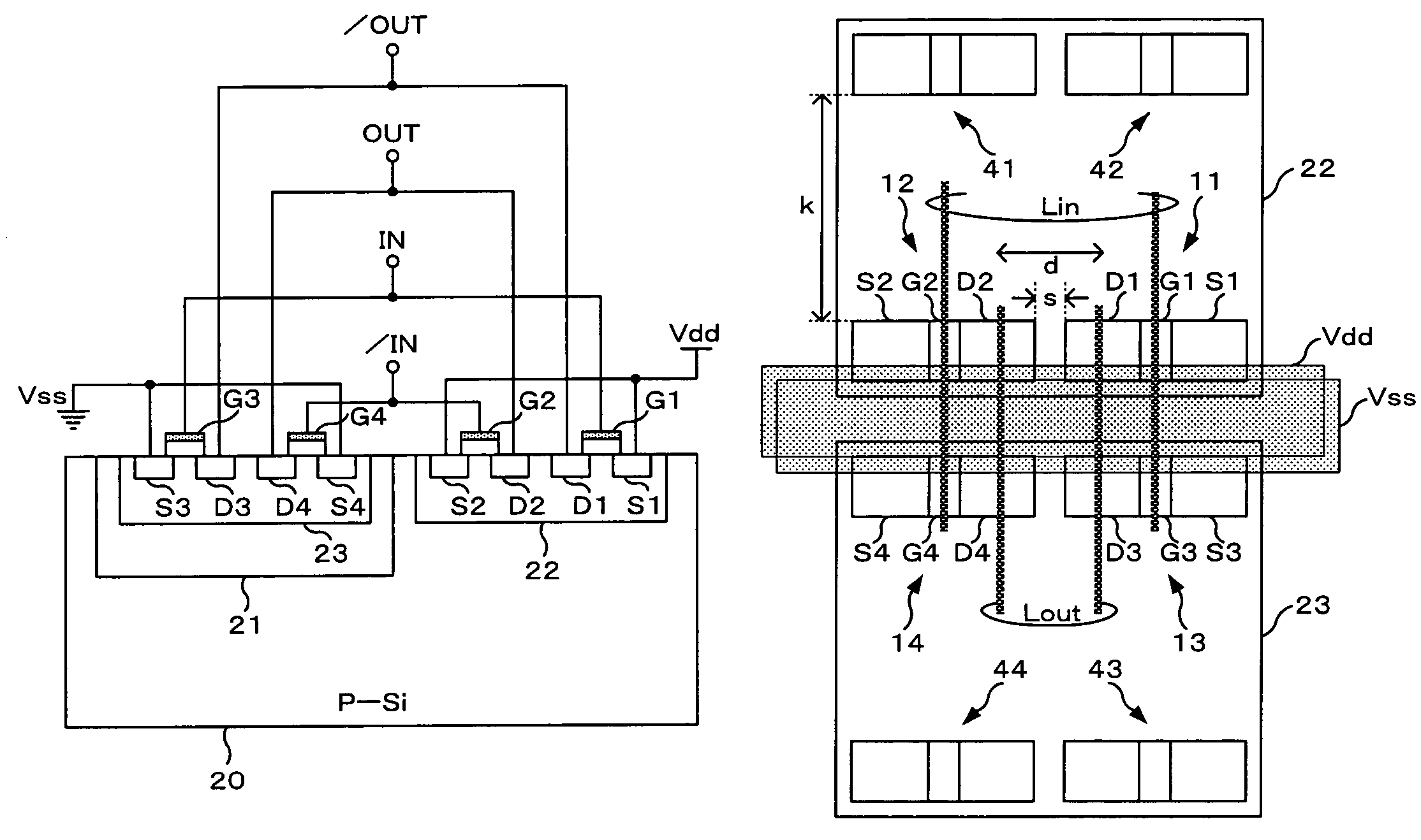
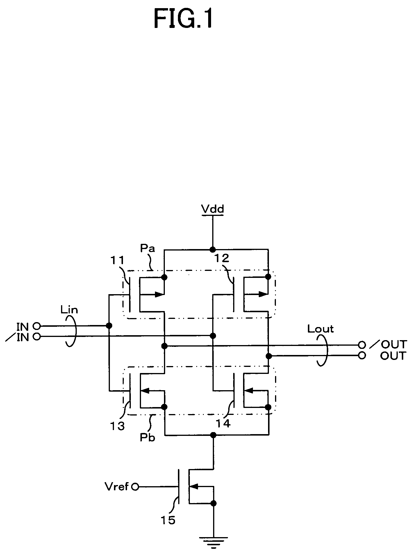
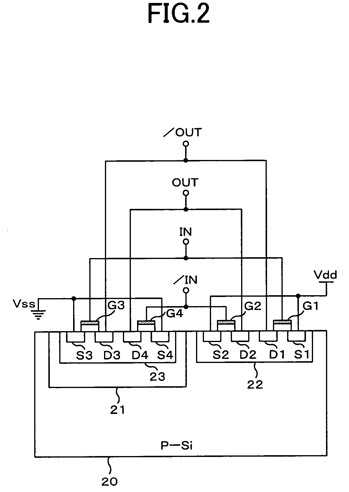
[0046]Described first is a case where the invention is applied to a differential driver circuit that is one example of the digital circuit comprised of MOS transistors. FIG. 1 is a circuit configuration diagram of the differential driver circuit as a basic structural example of the invention. The differential driver circuit as shown in FIG. 1 is comprised of PMOS transistors 11 and 12 and NMOS transistors 13, 14 and 15. Thus configured differential driver circuit receives paired high-frequency input signal IN and inverted input signal / IN via input transmission line Lin which is a paired structure of transmission line, while outputting paired output signal OUT and inverted output signal / OUT via output transmission line Lout which is a paired structure of transmission line.

[0047]In FIG. 1, an input signal IN is applied to gates of the PMOS transistor 11 and NMOS ...


PUM


Abstract

A semiconductor integrated circuit comprising: a pair of MOS transistors which are formed in a same well on a semiconductor substrate and arranged adjacent to each other with a distance such that charge exchange between capacitances of respective drain diffusion layers is possible; and a wiring structure which is formed to apply differential signals to respective gates of the pair of MOS transistors and to apply a common potential to respective sources of the pair of MOS transistors.

Description

BACKGROUND OF THE INVENTION[0001]1. Field of the Invention[0002]The present invention relates to a semiconductor integrated circuit, and more particularly, to a semiconductor integrated circuit configured to enable transmission of high-speed signals with frequencies of GHz in a digital circuit.[0003]2. Related Art[0004]In recent years, finer patterning has further proceeded in the semiconductor integrated circuit using MOS circuit. For example, the process of 0.18 μm has achieved widespread use, the process of 0.13 μm is coming into practical use, and the process of 0.09 μm has begun to be introduced. Further, with the patterning made finer in the semiconductor integrated circuit, requested is high-speed operation using high-frequency clocks, and demanded is the reliability of switching operation in a band of several GHz.[0005]Various attempts have been made to implement faster operation in the semiconductor integrated circuit. It is advantageous in increasing the operation speed to...

Claims


Application Information

Patent Timeline
Patent Type & Authority Patents(United States)
IPC IPC(8): H01L27/092
CPCG11C7/1051G11C7/1057H01L27/092
Inventor KAJIGAYA, KAZUHIKOOTSUKA, KANJI
Owner LONGITUDE LICENSING LTD
Why Eureka
Try Eureka