Organic thin film transistor

An organic thin film and transistor technology, applied in the field of organic thin film transistors, can solve problems such as limitations in productivity improvement, and achieve the effects of small performance degradation, excellent heat resistance, and excellent carrier mobility

Inactive Publication Date: 2016-10-12
FUJIFILM CORP
View PDF45 Cites 2 Cited by
  • Summary
  • Abstract
  • Description
  • Claims
  • Application Information

AI Technical Summary

Problems solved by technology

However, when an inorganic semiconductor is used to form the semiconductor layer of a TFT, a vacuum process and a high-temperature process of 300°C or higher are required, and there is a limit to the improvement of productivity.

Method used


Image

  • Organic thin film transistor
  • Organic thin film transistor
  • Organic thin film transistor

Examples


manufacture example 1

[0344] [Manufacturing Example 1] Fabrication of Bottom Gate OTFT-1

[0345]

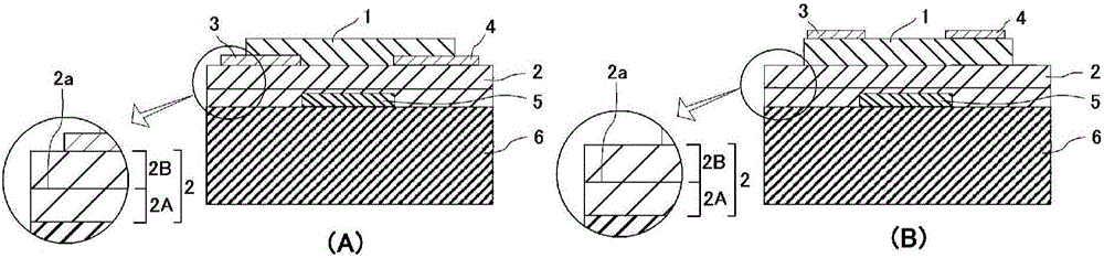
[0346] make figure 1 (A) Bottom-gate-bottom-contact OTFT of the form shown. As the substrate 6, a glass substrate with a thickness of 1.1 mm was used, and an ITO film with a thickness of 70 nm was formed thereon to form a gate electrode. A polyimide-based alignment film solution (SE-130, polyimide precursor solution, manufactured by Nissan Chemical Co. ), dried at 100°C for 10 minutes. Then, imidization was performed at 230° C. for 2 hours, whereby a polyimide film (thickness from the first insulating layer side surface of the gate electrode: 100 nm) was obtained. The surface of the film was subjected to rubbing treatment (orientation treatment) using a cotton cloth to form a first gate insulating layer.

[0347]

[0348]The polymerizable liquid crystal compound (liquid crystal monomer) shown in the table below and the polymerization initiator shown in the table below were dissolved in methyl...

manufacture example 2

[0377] [Manufacturing Example 2] Fabrication of Bottom Gate OTFT-2

[0378] On a glass substrate with a thickness of 1.1 mm, a polyimide-based alignment film solution (SE-130, polyimide precursor solution, Nissan Chemical Co. Manufacture), dried at 100°C for 10 minutes. Then, imidization was performed at 230° C. for 2 hours to form a polyimide film (thickness: 100 nm). The surface of the polyimide film was subjected to rubbing treatment (orientation treatment) using a cotton cloth, and an ITO film having a thickness of 70 nm was formed as a gate electrode on a part of the rubbing-treated surface. Then, a second gate insulating layer is formed to cover the gate electrode in the same manner as the formation of X1 described above.

[0379] On the second gate insulating layer, a source electrode, a drain electrode, and an organic semiconductor layer were formed in the same manner as in Manufacturing Example 1 to obtain an OTFT. The obtained OTFT is called OTFT Zt1.

manufacture example 3

[0380] [Manufacturing Example 3] Fabrication of Bottom Gate OTFT-3

[0381] In the above-mentioned Production Example 1, the following polymer liquid crystal compound (weight average molecular weight: 9300) having a repeating unit was used instead of the liquid crystal monomer, and alignment aging was carried out at 80°C, and the polymerization reaction was carried out by ultraviolet irradiation , except that the OTFT was produced in the same manner as in Production Example 1. The following polymer liquid crystal compounds exhibit a nematic phase at 60 to 90°C.

[0382] [chem 33]

[0383] polymer liquid crystal compound

[0384]

[0385] The obtained OTFT is called OTFT Zt2.


PUM


Abstract

A bottom-gate organic thin film transistor which comprises: a substrate; a gate electrode that is arranged on the substrate; a first gate insulating layer that is arranged so as to cover the gate electrode; a second gate insulating layer that is arranged on the first gate insulating layer; an organic semiconductor layer that is arranged on the second gate insulating layer; and a source electrode and a drain electrode, which are arranged in contact with the organic semiconductor layer and are connected to each other via the organic semiconductor layer. The second gate insulating layer-side surface of the first gate insulating layer is subjected to an alignment treatment, and the second gate insulating layer is obtained by polymerizing and immobilizing a polymerizable crystalline compound, which has been aligned in accordance with the alignment treatment, in the aligned state.

Description

technical field [0001] The present invention relates to organic thin film transistors. Background technique [0002] Many display devices such as liquid crystal displays, organic EL displays, and electrophoretic displays incorporate thin-film transistors (hereinafter also referred to as “TFTs”) as display switching devices. The TFT has a structure including a gate electrode, a semiconductor layer, and a gate insulating layer provided between the gate electrode and the semiconductor layer on a substrate, and furthermore, a source electrode and a drain electrode are provided in contact with the semiconductor layer. The TFT is driven by applying a voltage to the gate electrode. By applying a voltage to the gate electrode, the amount of carriers consisting of electrons or holes in the semiconductor is controlled, thereby controlling the current flowing between the source electrode and the drain electrode. [0003] Conventionally, inorganic semiconductors such as amorphous or p...

Claims


Application Information

Patent Timeline
Patent Type & Authority Applications(China)
IPC IPC(8): H01L29/786H01L51/05H01L51/30
CPCH10K71/191H10K85/623H10K85/6574H10K85/6576H10K85/40H10K10/474H01L29/786H10K10/466H10K10/471H10K10/478
Inventor 新居辉树
Owner FUJIFILM CORP
Why Eureka
Try Eureka