Light emitting element mounting member, and semiconductor device using the same

a technology of light emitting elements and mounting parts, which is applied in the direction of semiconductor lasers, lighting and heating apparatus, discharge tube luminescnet screens, etc., can solve the problems of increased temperature, increased raw material cost, and increased heat dissipation, and achieves efficient dissipation and superior cooling properties.

Active Publication Date: 2009-04-14
SUMITOMO ELECTRIC IND LTD
View PDF21 Cites 25 Cited by
  • Summary
  • Abstract
  • Description
  • Claims
  • Application Information

AI Technical Summary

Benefits of technology

[0007]The object of the present invention is to overcome the problems described above and to provide a light-emitting element mounting member and semiconductor device that uses the same that has high thermal conductivity and that is easy to process.
[0010]In a light-emitting element mounting member formed in this manner, the substrate serves as a high thermal conductivity member, thus allowing adequate dissipation of the heat generated by the semiconductor light-emitting element. Furthermore, since the reflective member contains metal, processing is made easier compared to a structure in which the reflective member is formed from ceramic. This makes it possible to provide a light-emitting element mounting member that is easier to process.
[0011]Also, since the reflective member contains metal, the bond with the metal layer disposed on the reflective surface of the reflective member improves. As a result, a light-emitting element mounting member that is easy to produce can be provided.
[0012]It would be preferable for the light-emitting element mounting member to further include a bonding layer bonding the element mounting surface and the reflective member. A heat resistance temperature of the bonding layer is at least 300 deg C. The bonding layer melts at a temperature of no more than 700 deg C. and bonds the element mounting surface and the reflective member. In this case, since the bonding layer has a heat resistance temperature of at least 300 deg C., the bonding layer can prevent peeling of the substrate and the reflective member and is practical even if the temperature when the semiconductor light-emitting element is mounted on the light-emitting element mounting member is 250-300 deg C. Thus, a highly reliable light-emitting element mounting member can be obtained. Furthermore, since the bonding temperature is no more than 700 deg C., if metallized patterns formed from Au, Ag or Al or the like are formed on the surface of the substrate, degradation of the metallized patterns can be prevented. Since the heat resistance temperature of these metallized patterns are generally no more than 700 deg C., the bonding can be performed without degradation of the metallized patterns by bonding at a temperature of no more than 700 deg C.
[0016]It would be preferable for an electrode to be disposed on the main surface side of the semiconductor light-emitting element and electrically connected to the first and / or the second conductor region. In this case, since the electrode is disposed on the main surface side and the electrode is directly connected electrically to the first and / or the second conductor region, the heat generated by the light-emission layer, which is the section of the semiconductor light-emitting element that especially generates heat, is transmitted directly to the substrate by way of the electrode. As a result, the heat generated by the light-emission layer is efficiently dissipated to the substrate, providing a light-emitting element mounting member with superior cooling properties. It would also be preferable for the main surface to have an area of at least 1 mm2.

Problems solved by technology

When a ceramic having aluminum oxide as its main component (hereinafter referred to also as alumina) is used in the substrate and the window frame, adequate heat dissipation is not possible, leading to increased temperature.
Furthermore, if aluminum nitride, which has high thermal conductivity, is used, the raw material is more expensive and harder to process than alumina.
With this method, however, thermal deformation and the like take place during firing, making it difficult to precisely form a metallized layer with a fine pattern, e.g., of less than 100 microns.

Method used


Image

  • Light emitting element mounting member, and semiconductor device using the same
  • Light emitting element mounting member, and semiconductor device using the same
  • Light emitting element mounting member, and semiconductor device using the same

Examples


first embodiment

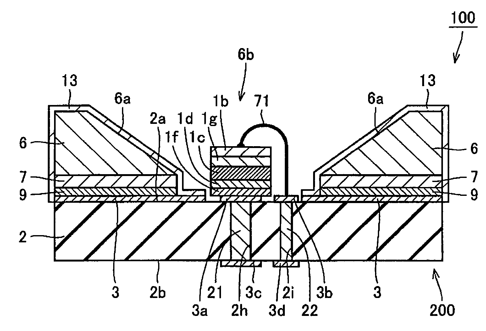
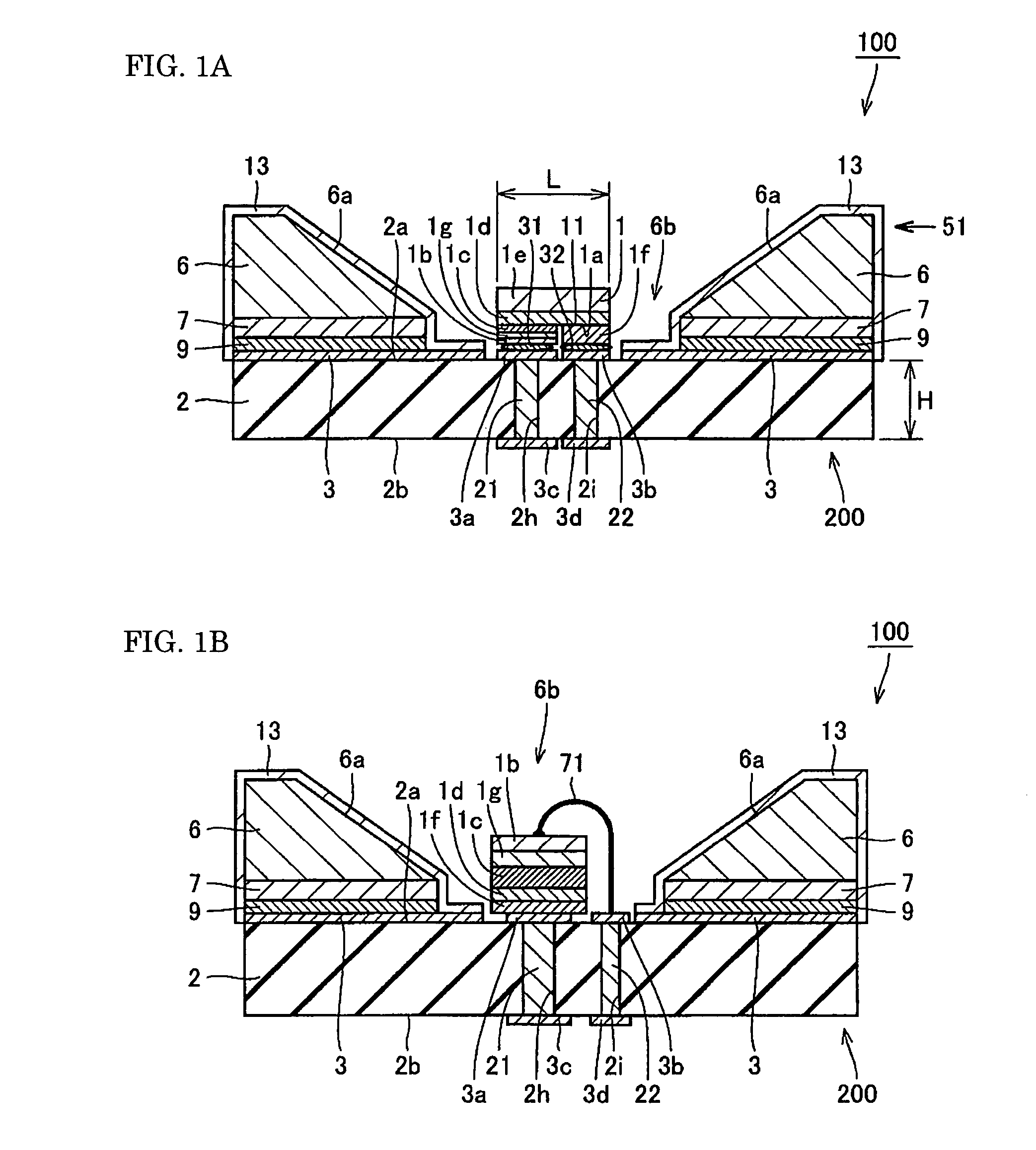
[0031]FIG. 1 is a cross-section drawing of a light-emitting element mounting member according to a first embodiment of the present invention and a semiconductor device using the same. FIG. 1A is a cross-section drawing of a semiconductor device according to one aspect. FIG. 1B is a cross-section drawing of a semiconductor device according to another aspect. FIG. 2 is a perspective drawing of the semiconductor device shown in FIG. 1A. FIG. 3 is a perspective drawing of the semiconductor light-emitting element shown in FIG. 1A. As shown in FIG. 1A, FIG. 2, and FIG. 3, a semiconductor device 100 according to the first embodiment of the present invention includes: a light-emitting element mounting member 200; and a semiconductor light-emitting element 1 mounted on an element mounting surface 2a. The semiconductor light-emitting element 1 includes a main surface 1a facing the element mounting surface 2a. In this example, the main surface 1a is formed as a rectangle including a longer fir...

second embodiment

[0069]FIG. 13 is a cross-section drawing of a light-emitting element mounting member and a semiconductor device that uses the same according to a second embodiment of the present invention. As shown in FIG. 13, in the light-emitting element mounting member 200 according to the second embodiment of the present invention, metal films 4, 4a, 4b are formed on the element mounting surface 2a, and the metal films 4, 4a, 4b are formed from Ag or Al. In this case, as shown in FIG. 13, it is possible to have the metal layer 13 formed only on the reflective member 6.

[0070]In this case, the same advantages are provided as those of the light-emitting element mounting member 200 and the semiconductor device 100 according to the first embodiment.

working example

[0071]A detailed study into the characteristics of the bonding layer 9 bonding the substrate 2 and the reflective member 6 was performed using a working example. Referring to FIG. 1, the reflective member 6 was attached to the element mounting surface 2a of the substrate 2 formed from aluminum nitride, interposed by the bonding layer 9. The reflective member 6 is an Ni—Co—Fe alloy with an Ni proportion of 29% by mass, a Co proportion of 18% by mass, and an Fe proportion of 53% by mass. Also, the dimensions of the reflective member 6 were set to 5 mm×5 mm×1 mm (height×width×thickness).

[0072]For the bonding layer 9, the sample 1 through the sample 8 from Table 1 were used.

[0073]

TABLE 1ElectrodemetallizedHeatHeatpatternSampleMaterial for theBondingresistanceresistancedegradationNo.bonding layer 9temperature12Strength(Au film 3)Notes1SolderAu—Ge 12%360° C.◯◯◯◯⊚2Ag—Cu 28%780° C.◯◯◯XDiscoloration in Au immediatelyafter bonding; Film thicknessreduced3Au—Sn 20%280° C.XX◯◯Re-melting of bondi...


PUM


Abstract

The object of the present invention is to provide a light-emitting element mounting member and a semiconductor device using the same that is easy to process and that allows adequate heat dissipation.A light-emitting element mounting member 200 includes: a substrate 2 including an element mounting surface 2a mounting a semiconductor light-emitting element 1 and first and second conductive regions 21, 22 disposed on the element mounting surface 2a and connected to the semiconductor light-emitting element 1; a reflective member 6 including a reflective surface 6a defining an internal space 6b for housing the semiconductor light-emitting element 1 and containing a metal disposed on the element mounting surface 1a; and a metal layer 13 disposed on the reflective surface 6a. The reflective surface 6a is sloped relative to the element mounting surface 2a so that a diameter of the internal space 6b is greater away from the element mounting surface 2a.

Description

CROSS-REFERENCE TO PRIOR APPLICATION[0001]This is a U.S. National Phase application under 35 U.S.C. §371 of International Patent Application No. PCT / JP2004 / 003443 filed Mar. 15, 2004, and claims the benefit of Japanese Patent Application No. 2003-074036, filed March 18, 2003, both of which are incorporated by reference herein. The International Application was published in Japanese on Sep. 30, 2004 as WO 2004 / 084319 A1 under PCT Article 21(2).TECHNICAL FIELD[0002]The present invention relates to a light-emitting element mounting member and a semiconductor device using the same. More specifically, the present invention relates to a light-emitting mounting element for mounting a light-emitting diode, a semiconductor laser, or the like and a semiconductor device using the same.BACKGROUND ART[0003]An example of a conventional member for mounting semiconductor light-emitting elements is described in Japanese Laid-Open Patent Publication Number 2002-232017.[0004]In the semiconductor mount...

Claims


Application Information

Patent Timeline
Patent Type & Authority Patents(United States)
IPC IPC(8): H01L33/00H01L33/60H01L33/62H01L33/64H01S5/00H01S5/02H01S5/022
CPCH01L33/60H01L33/486H01S5/0224H01S5/02292H01L2224/48091H01L2224/48465H01L2224/73265H01L2924/00014H01L2224/16225H01L2924/00H01L2224/05573H01L2224/05568H01L2224/05644H01L2224/06102H01L2224/1703H01L24/05H01S5/0234H01S5/02255
Inventor ISHIDU, SADAMUHIGAKI, KENJIROISHII, TAKASHITSUZUKI, YASUSHI
Owner SUMITOMO ELECTRIC IND LTD
Why Eureka
Try Eureka