Semiconductor device having a pseudo power supply wiring

a technology of pseudo power supply and semiconductor device, which is applied in the direction of electronic switching, reliability increasing modifications, electrical apparatus, etc., can solve the problems of disadvantageous sub-threshold current flowing through the transistor in an off state, fundamentally difficult to render the transistor size small, and signal is slightly delayed, so as to reduce power consumption and reduce switching speed

Active Publication Date: 2009-05-12
LONGITUDE LICENSING LTD
View PDF23 Cites 10 Cited by
  • Summary
  • Abstract
  • Description
  • Claims
  • Application Information

AI Technical Summary

Benefits of technology

[0015]The present invention has been achieved to solve such problems. It is therefore an object thereof to provide a semiconductor device capable of further reducing power consumption at the time of standby state while suppressing a decrease in switching speed from a standby state to an active state.
[0021]According to the present invention, as a transistor that connects a main power supply wiring and an pseudo power supply wiring, both an N-channel MOS transistor and a P-channel MOS transistor are used, and the both transistors are rendered a conductive state at the time of active state. Thus, it becomes possible to reduce power consumption at the time of standby while suppressing a decrease in switching speed from a standby state to an active state.
[0023]Thus, according to the present invention, it becomes possible to reduce power consumption at the time of standby while suppressing a decrease in switching speed from the standby state to the active state.

Problems solved by technology

As a result, a sub-threshold current flowing through the transistor in an off state disadvantageously increases.
Thus, it is fundamentally difficult to render the transistor size small.
However, when the signal is passed through the level conversion circuit, the signal is slightly delayed.
As a result, there occurs another problem in that a timing of switching the circuit block 10 from the standby state to the active state is delayed.

Method used


Image

  • Semiconductor device having a pseudo power supply wiring
  • Semiconductor device having a pseudo power supply wiring
  • Semiconductor device having a pseudo power supply wiring

Examples


first embodiment

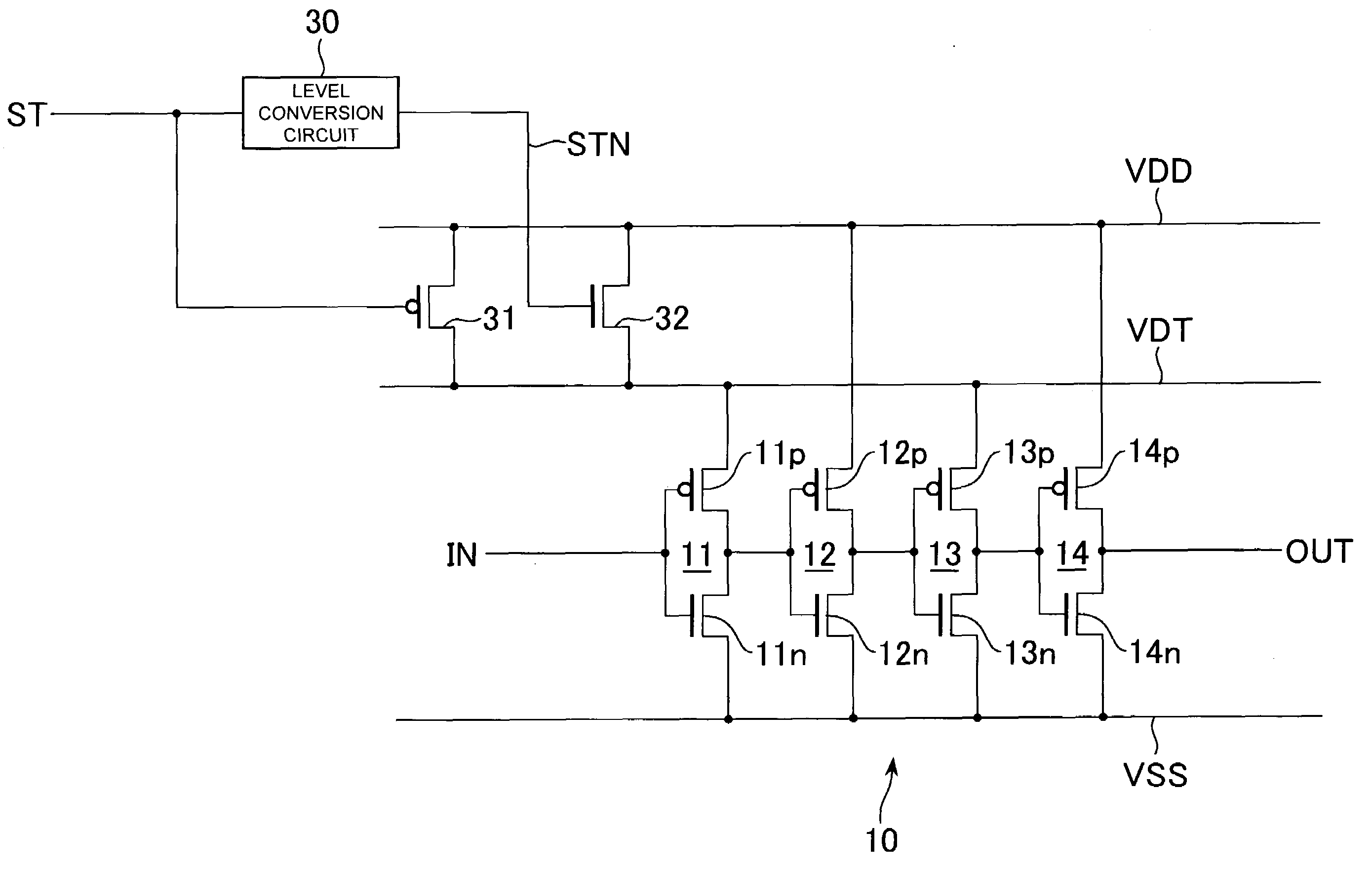
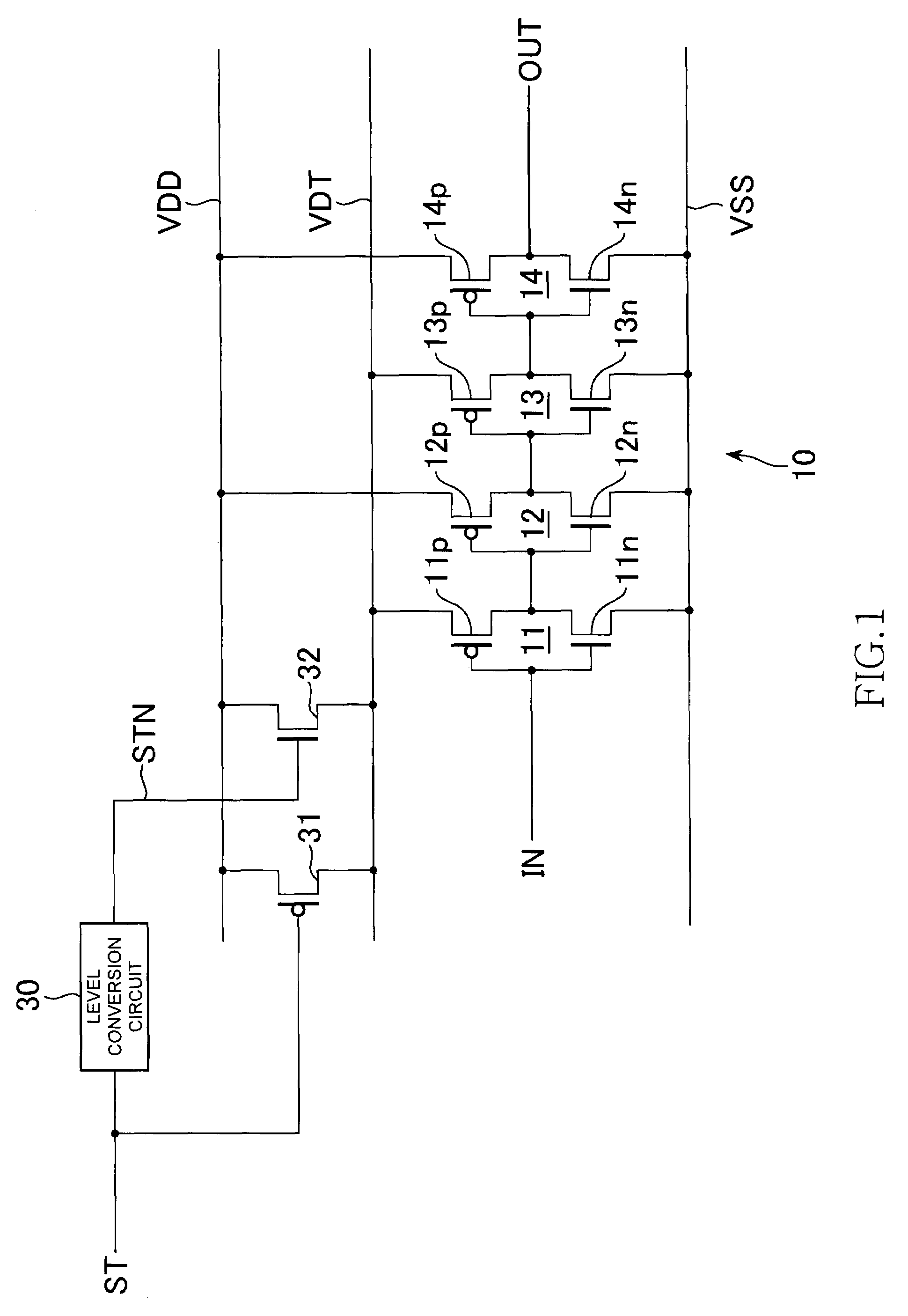
[0033]FIG. 1 is a circuit diagram of a semiconductor device according to the present invention.

[0034]As shown in FIG. 1, the semiconductor device includes the circuit block 10 configured of 4-stage inverters 11 to 14, similar to the conventional circuit shown in FIG. 7. In the circuit block 10, logic is fixed at the time of standby state, and its input signal IN is fixed to a high level at the time of standby state. Out of the four inverters 11 to 14 included in the circuit block 10, the first-stage inverter 11 and the third-stage inverter 13 are connected between the pseudo power supply wiring VDT and the main power supply wiring VSS, and the second-stage inverter 12 and the fourth-stage inverter 14 are connected between the main power supply wiring VDD and the main power supply wiring VSS.

[0035]In the present embodiment, three power wirings, that is, the main power supply wiring VDD, the pseudo power supply wiring VDT, and the main power supply wiring VSS are arranged. In the pres...

second embodiment

[0047]the present invention is described next.

[0048]FIG. 3 is a circuit diagram of a semiconductor device according to the second embodiment of the present invention.

[0049]As shown in FIG. 3, the semiconductor device according to the present embodiment further includes an pseudo power supply wiring VST and an N-channel MOS transistor 41 arranged between the main power supply wiring VSS and the pseudo power supply wiring VST. A gate electrode of the N-channel MOS transistor 41 is supplied via an inverter INV with an inverted standby signal STB.

[0050]In the present embodiment, out of the four inverters 11 to 14 included in the circuit block 10, the first-stage inverter 11 and the third-stage inverter 13 are connected between the pseudo power supply wiring VDT and the main power supply wiring VSS, and the second-stage inverter 12 and the fourth-stage inverter 14 are connected between the main power supply wiring VDD and the pseudo power supply wiring VST. Since other configurations are...

third embodiment

[0054]the present invention is described next.

[0055]FIG. 4 is a circuit diagram of a semiconductor device according to the third embodiment of the present invention.

[0056]As shown in FIG. 4, the semiconductor device of the present embodiment differs from the semiconductor device according to the second embodiment shown in FIG. 3 in that the former includes: a P-channel MOS transistor 42 connected between the main power supply wiring VSS and the pseudo power supply wiring VST; and a level conversion circuit 40 that supplies a standby signal STP to a gate electrode of the P-channel MOS transistor 42. Since other configurations are the same as those in the second embodiment, the same parts are designated by the same reference numerals, and redundant descriptions thereof will be omitted.

[0057]In the present embodiment, a large difference is given between a drive capability of the N-channel MOS transistor 41 and that of the P-channel MOS transistor 42. That is, similar to the P-channel M...


PUM


Abstract

A semiconductor device includes main power supply wirings VDD and VSS, an pseudo power supply wiring VDT, inverters connected between the pseudo power supply wiring VDT and the main power supply wiring VSS, and inverters connected between the main power supply wiring VDD and the main power supply wiring VSS. Between the main power supply wiring VDD and the pseudo power supply wiring VDT, an N-channel MOS transistor and a P-channel MOS transistor that are rendered a conductive state at the time of active are connected in parallel. According to the present invention, the transistors different in conductivity type are used in parallel, and thus, it becomes possible to reduce power consumption at the time of standby while suppressing a decrease in switching speed from a standby state to an active state.

Description

TECHNICAL FIELD[0001]The present invention relates to a semiconductor device, and particularly relates to a semiconductor device the power consumption of which can be reduced in a standby state.BACKGROUND OF THE INVENTION[0002]In recent years, an operating voltage of a semiconductor device has been gradually decreasing so as to reduce power consumption of the semiconductor device. Currently, some semiconductor devices use quite low operating voltages of about 1 volt. If the operating voltage decreases, it is necessary to reduce a threshold voltage of each transistor accordingly. As a result, a sub-threshold current flowing through the transistor in an off state disadvantageously increases. To solve such a problem, a method of dividing power supply wirings into a main power supply wiring and a pseudo power supply wiring have been proposed in Japanese Patent Application Laid-open Nos. 2000-13215 and 2000-48568.[0003]FIG. 7 is a circuit diagram of a conventional semiconductor device us...

Claims


Application Information

Patent Timeline
Patent Type & Authority Patents(United States)
IPC IPC(8): H03K19/096H03K19/003
CPCH03K19/0016
Inventor FUJIKAWA, ATSUSHINODA, HIROMASA
Owner LONGITUDE LICENSING LTD
Why Eureka
Try Eureka