Conductive adhesive for thinned silicon wafers with through silicon vias

a technology of thinned silicon and conductive adhesive, which is applied in the testing/measurement of individual semiconductor devices, semiconductor/solid-state devices, instruments, etc., can solve the problems of conductive features and damage to the circuits present on the wafer, and achieve the effect of avoiding electrostatic discharg

Active Publication Date: 2009-06-02
IBM CORP
View PDF12 Cites 35 Cited by
  • Summary
  • Abstract
  • Description
  • Claims
  • Application Information

AI Technical Summary

Benefits of technology

[0010]Use of an electrically conductive adhesive for attachment of the mechanical handler to the thinned silicon wafer allows for electrical testing to verify that the TSVs are conductive. Testing can also be conducted for shorts, leakage and circuit function. The processing, handling and testing of the thinned silicon wafer can be conducted while the wafer is grounded. This protects the wafer by avoiding electrostatic discharge. Electrostatic discharge can cause damage to the circuits present on the wafer and the conductive features present on the wafer, or on a die on the wafer.

Problems solved by technology

Electrostatic discharge can cause damage to the circuits present on the wafer and the conductive features present on the wafer, or on a die on the wafer.

Method used


Image

  • Conductive adhesive for thinned silicon wafers with through silicon vias
  • Conductive adhesive for thinned silicon wafers with through silicon vias

Examples


Embodiment Construction

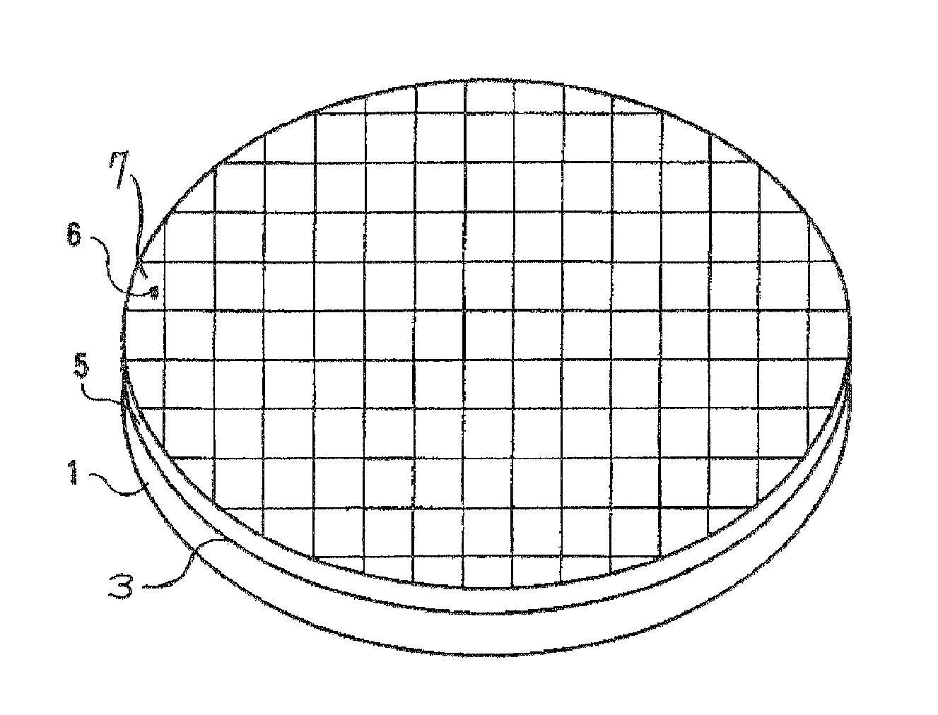
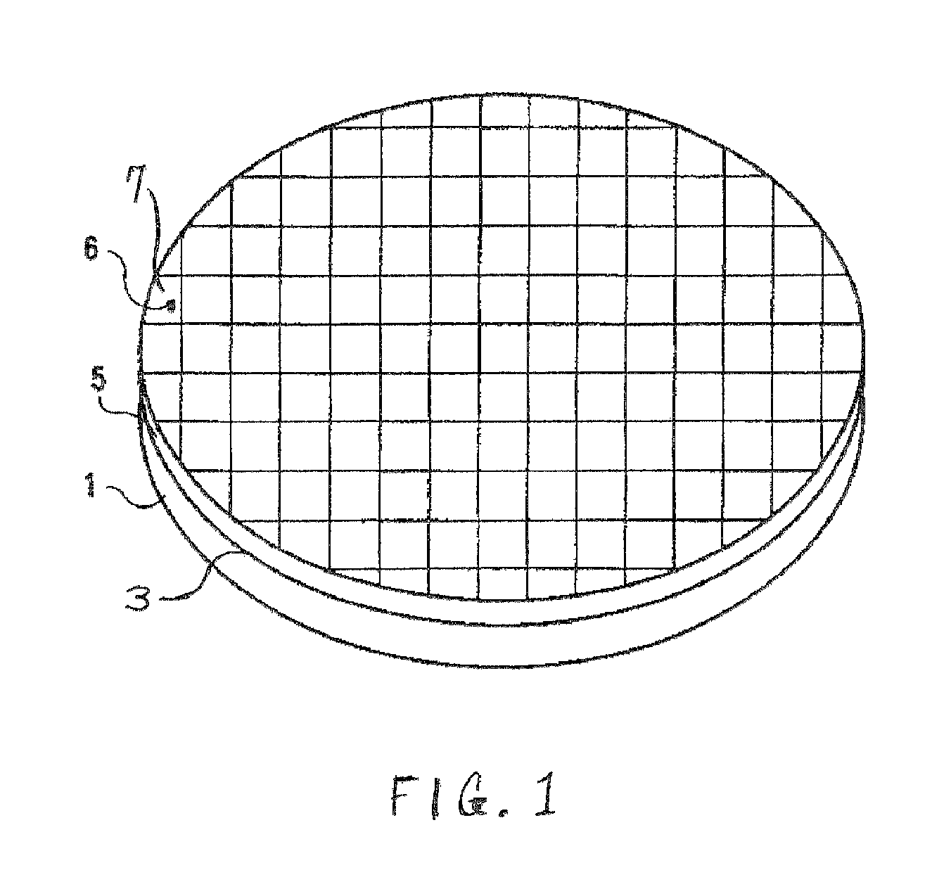
[0012]An embodiment of the present invention is a process for the use of an electrically conductive adhesive composition for performing electrical testing or burn-in test evaluations on thinned silicon wafers containing TSV and circuit designs. The testing of the thinned silicon wafer, the thinned silicon die, the thinned silicon stacked die or the thinned silicon stacked wafer can be performed without damage to the die or wafer. Since the adhesive material is conductive, testing can be performed on either side of the wafers. Testing can be performed on the through-silicon vias (TSVs). The electrically conductive adhesive can also be thermally conductive. It is therefore effective in enhanced heat dissipation during wafer testing.

[0013]Electrically conductive adhesive compositions include polymeric materials that contain conductive fillers. Epoxy polymeric adhesives containing an electrically conductive filler are examples of conductive adhesives. Other examples of conductive adhesi...


PUM


Abstract

The present invention relates to a process for preparing a thinned silicon wafer for electrical testing, the thinned silicon wafer comprising at least one circuit design and at least one through-silicon via or hole; the process comprising temporarily attaching the thinned silicon wafer to a mechanical handler by means of an electrically conductive polymeric adhesive material.

Description

[0001]The present invention relates to a process for performing electrical testing and reliability screening on semiconductor wafers; and particularly to a process for testing thinned silicon wafers that contain through-silicon vias (TSVs) or holes.BACKGROUND OF THE INVENTION[0002]Semiconductor manufacturers who make integrated circuit chips begin by manufacturing semiconductor wafers. Each wafer is typically 100 mm, 125 mm, 150 mm, 200 mm or 300 mm in diameter and contains anywhere from one to several thousand chips or die on the wafer. When manufacture of the wafer is completed, chips or die are cut or “diced” from the wafer and may later be mounted into single chip or multiple chip packages for implementation in a printed circuit board or other applications.[0003]When manufacture of a wafer is completed, and before the chips or die are cut or “diced” from the wafer, it is customary practice to test each chip on the wafer to determine whether each chip, as manufactured, electrical...

Claims


Application Information

Patent Timeline
Patent Type & Authority Patents(United States)
IPC IPC(8): H01L21/00
CPCH01L21/67132H01L22/14H01L21/2007H01L2924/0002H01L2924/00
Inventor KNICKERBOCKER, JOHN U
Owner IBM CORP
Why Eureka
Try Eureka