Electron emission display including a cathode having resistance layer electrically connecting isolation electrodes having electron emission regions to a line electrode

a technology of electron emission region and resistance layer, which is applied in the manufacture of electrode systems, electric discharge tubes/lamps, and discharge tubes luminescent screens, etc., can solve the problems of difficult to achieve high resolution display screens, inevitably occurring voltage drop, and deterioration of light emission uniformity per respective pixels, so as to reduce resistance, widen the effective width of the first electrode, and increase the emission characteristics of electron emission regions.

Inactive Publication Date: 2009-06-02
SAMSUNG SDI CO LTD
View PDF9 Cites 0 Cited by
  • Summary
  • Abstract
  • Description
  • Claims
  • Application Information

AI Technical Summary

Benefits of technology

[0014]It is an aspect of the present invention to provide an improved electron emission device that has a resistance layer on a plurality of first electrodes to make the emission characteristics of the electron emission regions more uniform, and that widens the effective width of the first electrodes to reduce resistance and achieves a high resolution display screen.

Problems solved by technology

In this case, the emission characteristics of the electron emission regions become non-uniform so that light emission uniformity per respective pixels is deteriorated.
Accordingly, with the above-structured electron emission device, a voltage drop inevitably occurs due to the increase in resistance pursuant to the reduction in an effective width.
In the case that the effective width is enlarged to lower the resistance, it is difficult to achieve a high resolution display screen due to the enlargement in the width of the first electrodes.

Method used


Image

  • Electron emission display including a cathode having resistance layer electrically connecting isolation electrodes having electron emission regions to a line electrode
  • Electron emission display including a cathode having resistance layer electrically connecting isolation electrodes having electron emission regions to a line electrode
  • Electron emission display including a cathode having resistance layer electrically connecting isolation electrodes having electron emission regions to a line electrode

Examples


Embodiment Construction

[0030]In the following detailed description, only certain exemplary embodiments of the present invention are shown and described, by way of illustration. As those skilled in the art would recognize, the described exemplary embodiments may be modified in various ways, all without departing from the spirit or scope of the present invention. Accordingly, the drawings and description are to be regarded as illustrative in nature, and not restrictive.

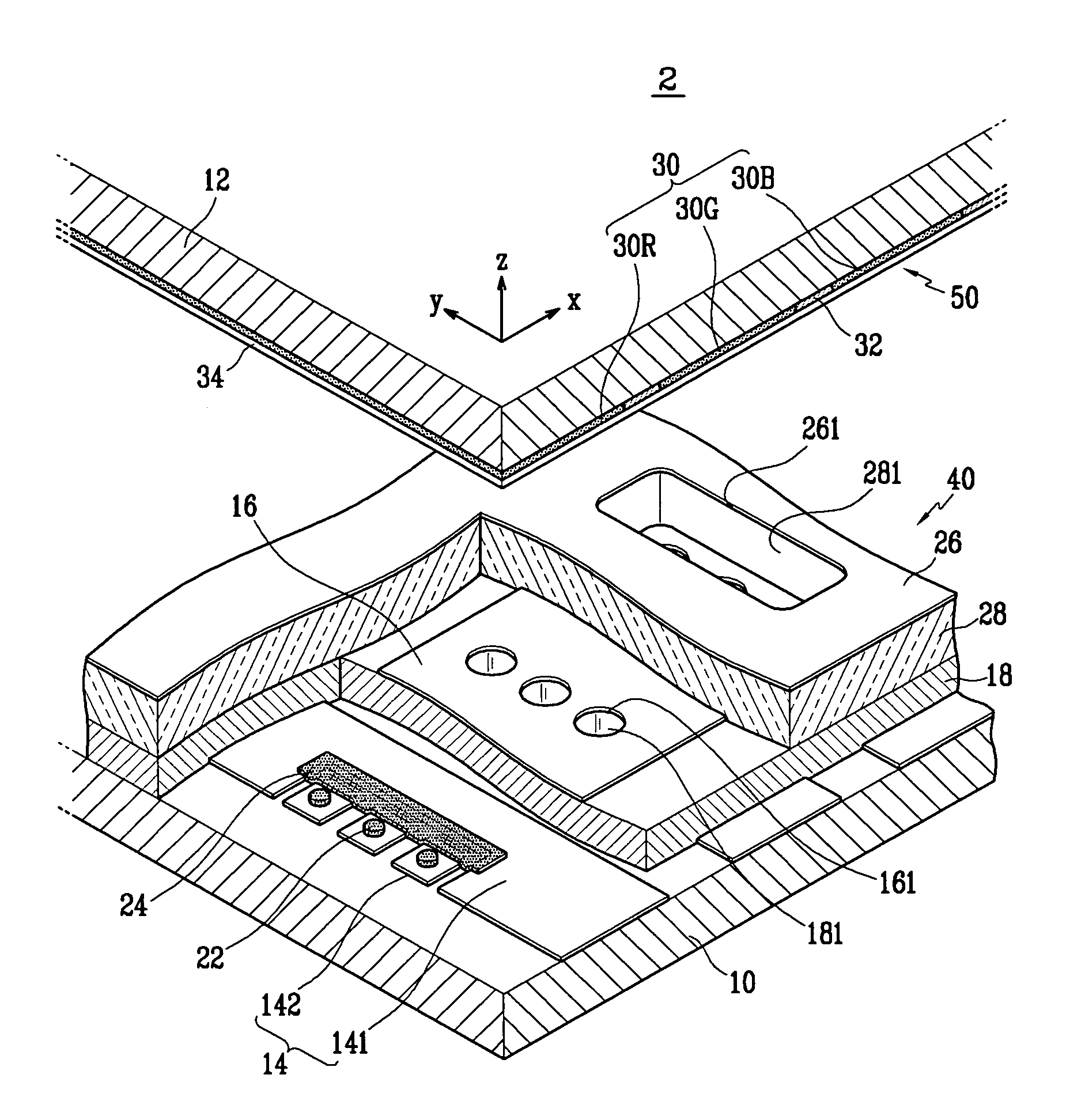
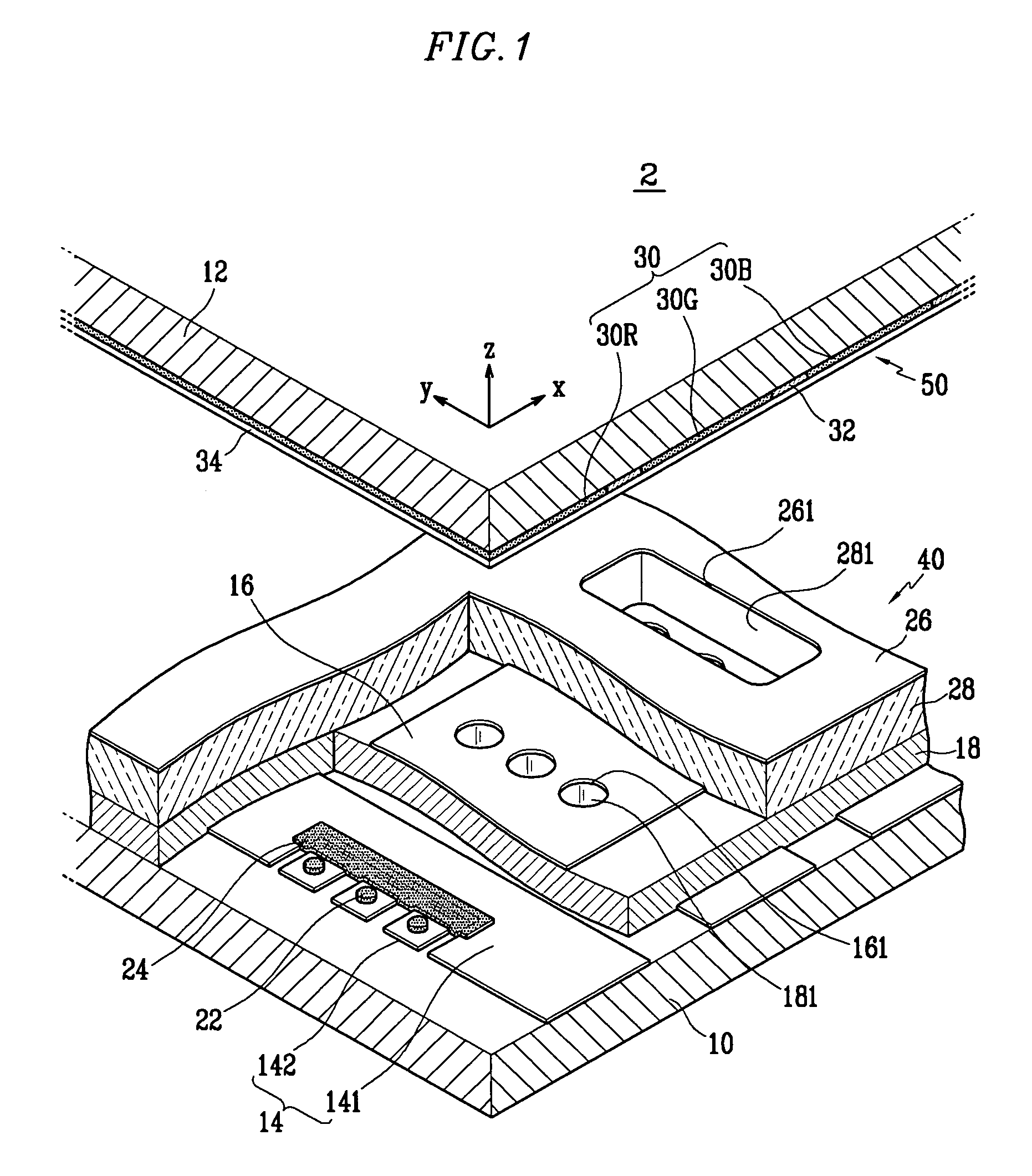
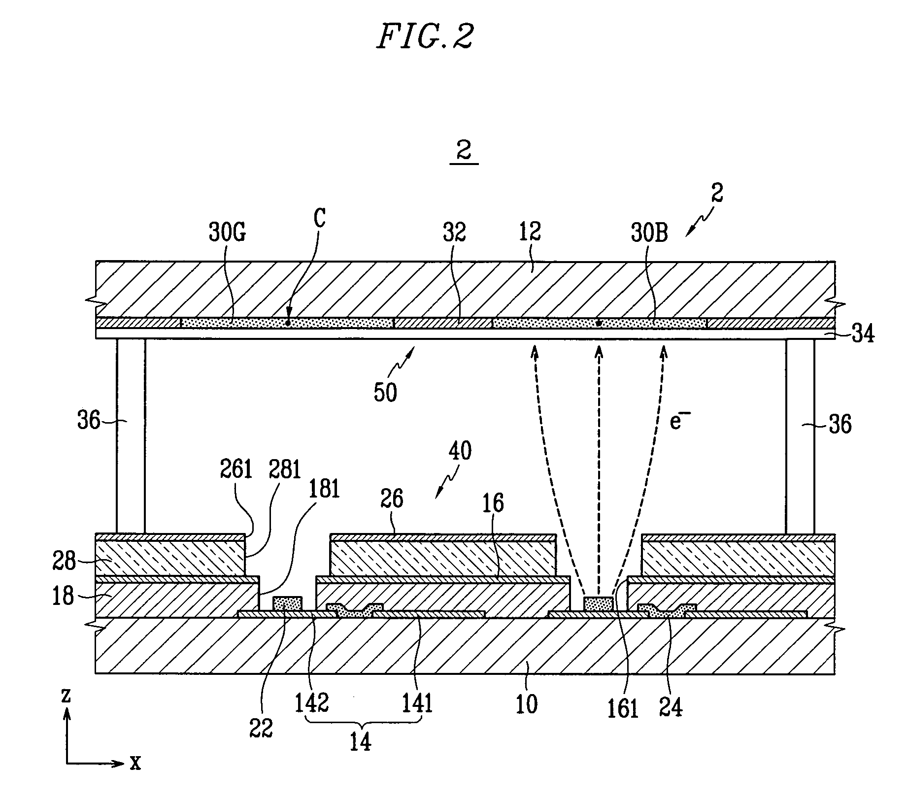
[0031]FIGS. 1 and 2 are a partial exploded perspective view and a partial sectional view of an electron emission display 2 according to a first embodiment of the present invention, and FIG. 3 is a partial plan view of an electron emission device according to the first embodiment of the present invention.

[0032]As shown in FIGS. 1, 2, and 3, the electron emission display 2 includes a first substrate 10, and a second substrate 12 facing the first substrate 10 in parallel with a distance therebetween (wherein the distance therebetween may be pred...


PUM


Abstract

An electron emission device includes a substrate, cathode and gate electrodes placed on the substrate in an insulated manner, and electron emission regions electrically connected to the cathode electrodes. Each of the cathode electrodes includes a line electrode having a groove at one lateral side surface thereof, and isolation electrodes formed on the substrate exposed through the groove such that the isolation electrodes are isolated from the line electrode. The electron emission regions are placed on the isolation electrodes and a resistance layer electrically connects the isolation electrodes to the line electrode.

Description

CROSS-REFERENCE TO RELATED APPLICATION[0001]The application claims priority to and the benefit of Korean Patent Application No. 10-2005-0091988, filed on Sep. 30, 2005, in the Korean Intellectual Property Office, the entire content of which is incorporated herein by reference.BACKGROUND OF THE INVENTION[0002]1. Field of the Invention[0003]The present invention relates to an electron emission device, and in particular, to an electron emission display that reduces a resistance by widening an effective width of driving electrodes, and improves a shape of the driving electrodes to achieve a high resolution display screen.[0004]2. Description of Related Art[0005]In general, an electron emission element can be classified, depending upon the kinds of electron sources, into a hot cathode type or a cold cathode type.[0006]Among the cold cathode type of electron emission elements, there are a field emitter array (FEA) type, a surface conduction emission (SCE) type, a metal-insulator-metal (MI...

Claims


Application Information

Patent Timeline
Patent Type & Authority Patents(United States)
IPC IPC(8): H01J1/14H01J1/13H01J19/06H01J19/02H01J1/62H01J63/04
CPCH01J1/30H01J1/304H01J29/04H01J31/127
Inventor CHO, JIN-HUILEE, SANG-JOJEON, SANG-HOAHN, SANG-HYUCKHONG, SU-BONGJEA, BYUNG-GIL
Owner SAMSUNG SDI CO LTD
Why Eureka
Try Eureka