Low power, race free programmable logic arrays

Inactive Publication Date: 2009-06-02
ARIZONA STATE UNIVERSITY
View PDF8 Cites 7 Cited by
  • Summary
  • Abstract
  • Description
  • Claims
  • Application Information

AI Technical Summary

Benefits of technology

[0022]The combination of the PLA architecture of the present invention and embedding the PLA clock into the AND plane input signals effectively removes any race conditions, which would result in a fault in the OR plane and thus a fault in the output of the PLA. The present invention also reduces power consumption relative to the PLA architectures of the prior art. In particular, the use of series-connected transistor stacks in the NAND blocks of the AND plane, and perhaps in the transistor stacks of the OR plane, minimizes the amount of leakage current and hence the keeper current necessary to maintain various nodes in the AND and OR planes at high levels. Further, the use of NAND logic in the AND plane may result in the AND plane looking like a large AND gate. As such, an assertion from the AND plane is asserted from a normally low state to a high state, saving further power.

Problems solved by technology

Further, the use of NAND logic in the AND plane may result in the AND plane looking like a large AND gate.

Method used


Image

  • Low power, race free programmable logic arrays
  • Low power, race free programmable logic arrays
  • Low power, race free programmable logic arrays

Examples


Embodiment Construction

[0040]The embodiments set forth below represent the necessary information to enable those skilled in the art to practice the invention and illustrate the best mode of practicing the invention. Upon reading the following description in light of the accompanying drawing figures, those skilled in the art will understand the concepts of the invention and will recognize applications of these concepts not particularly addressed herein. It should be understood that these concepts and applications fall within the scope of the disclosure and the accompanying claims.

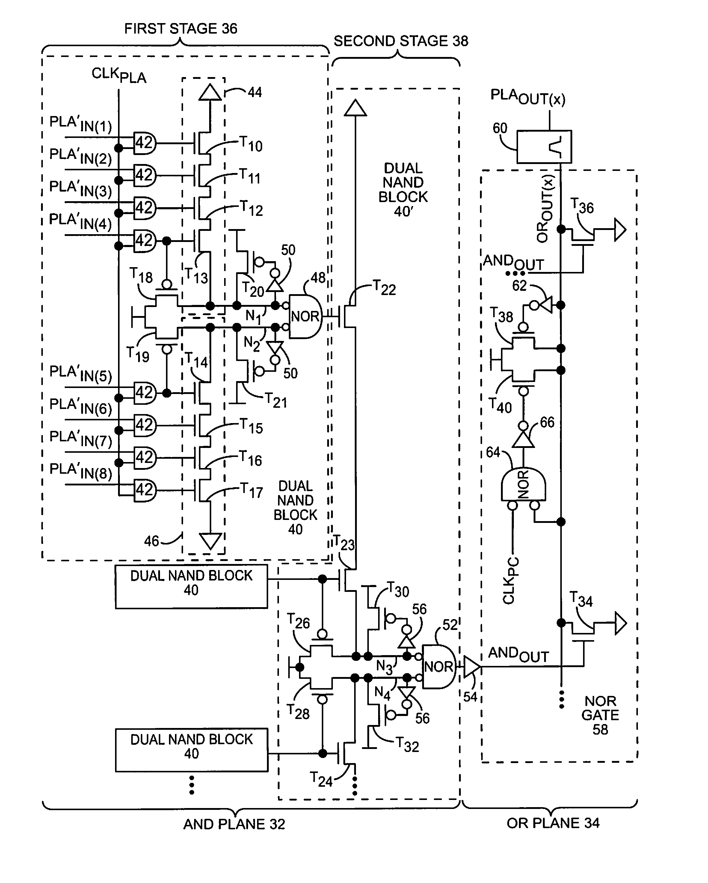
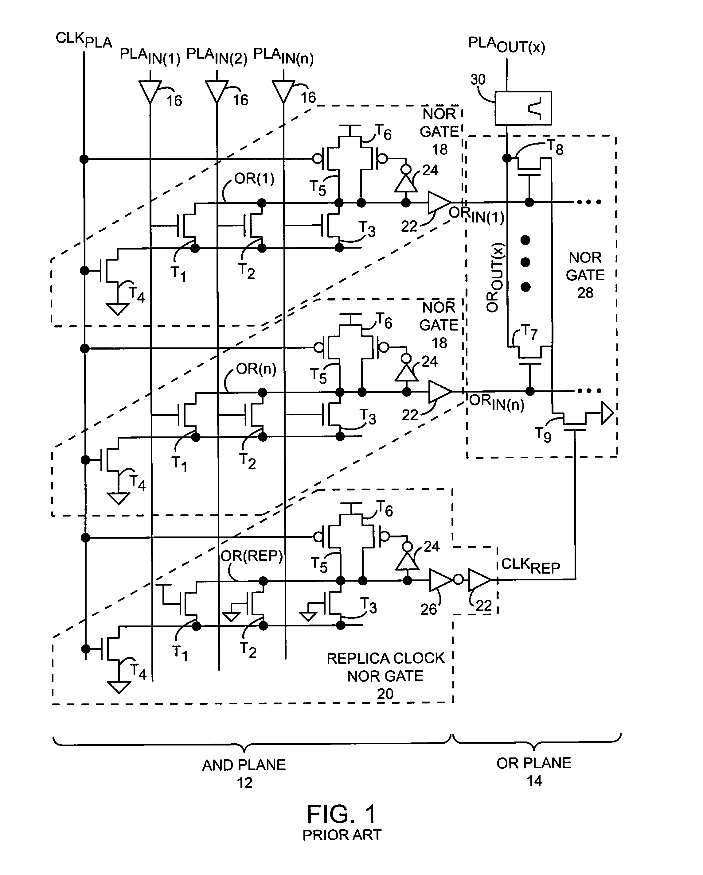
[0041]The present invention provides a PLA architecture that avoids the race condition and excessive leakage current of the prior art, especially relative to NOR-NOR PLA structures. In contrast to the prior art, the present invention provides a NAND-NOR PLA structure. A logical representation of a portion of an exemplary NAND-NOR PLA structure is provided in FIG. 4 according to one embodiment of the present invention. Like other P...


PUM


Abstract

The present invention provides a PLA architecture where the AND plane is implemented with NAND logic. The OR plane may be implemented with various logic, but in one embodiment, the OR plane is implemented with NOR logic. The AND plane may have multiple sequential stages providing hierarchical NAND logic. The NAND logic may be broken into a hierarchy of NAND logic blocks. Each NAND logic block may include one or more series-connected NAND transistor stacks. Each transistor in the transistor stack may receive an input signal representing the product of a PLA clock signal and either a direct PLA input or the complement thereof. As such, the PLA clock is inherently integrated with the input signals that drive the various transistors of the NAND transistor stacks.

Description

FIELD OF THE INVENTION[0001]The present invention relates to programmable logic arrays (PLAs), and in particular to low power PLAs that are free of potential timing races.BACKGROUND OF THE INVENTION[0002]Those skilled in the art will recognize that PLAs are generally broken into two planes. Input signals are presented to an AND plane, which determines the products of the input signals to generate product terms. The product terms are presented to the OR plane, which will determine the sum of the product terms that were provided by the AND plane. The output of the OR plane is latched for use by other circuitry or fed back into an input of the AND plane. Accordingly, PLAs provide a sum-of-products based on available inputs. Any logic function can be expressed in a sum-of-products form, wherein each output is the sum of products of true or complementary inputs.[0003]Conventionally, dynamic NOR gates have been used to implement both the AND plane and the OR plane. Dynamic logic gates are...

Claims


Application Information

Patent Timeline
IPC IPC(8): H03K19/177
CPCH03K19/1772
Inventor CLARK, LAWRENCE T.SAMSON, GIBY
Owner ARIZONA STATE UNIVERSITY
Why Eureka
Try Eureka