Frequency multiplier

a frequency multiplier and frequency technology, applied in the field of frequency multipliers, can solve the problems of low signal intensity of frequency-doubled components, large circuit scale and current consumption, and difficult extraction, and achieve the effect of low current consumption, effective utilization of frequencies, and simple circuit configuration

Inactive Publication Date: 2009-06-09
SOCIONEXT INC
View PDF18 Cites 7 Cited by
  • Summary
  • Abstract
  • Description
  • Claims
  • Application Information

AI Technical Summary

Benefits of technology

[0019]The present invention has been made to solve the above problems in the related art, and an object of the invention is therefore to provide a frequency multiplier capable of switching as appropriate among frequency signals hav

Problems solved by technology

This results in a problem that even-numbered harmonic components such as a frequency-doubled component have low signal intensity and hence are hard to extract.
It is unavoidable that the circuit scale and the current consumption become large.
This is problematic when the frequency multiplier 100 is applied to, for example, portable equipment such as cellular phones, because neither high-density mounting nor low power consumption can be attained.
There are probl

Method used


Image

  • Frequency multiplier
  • Frequency multiplier
  • Frequency multiplier

Examples


first embodiment

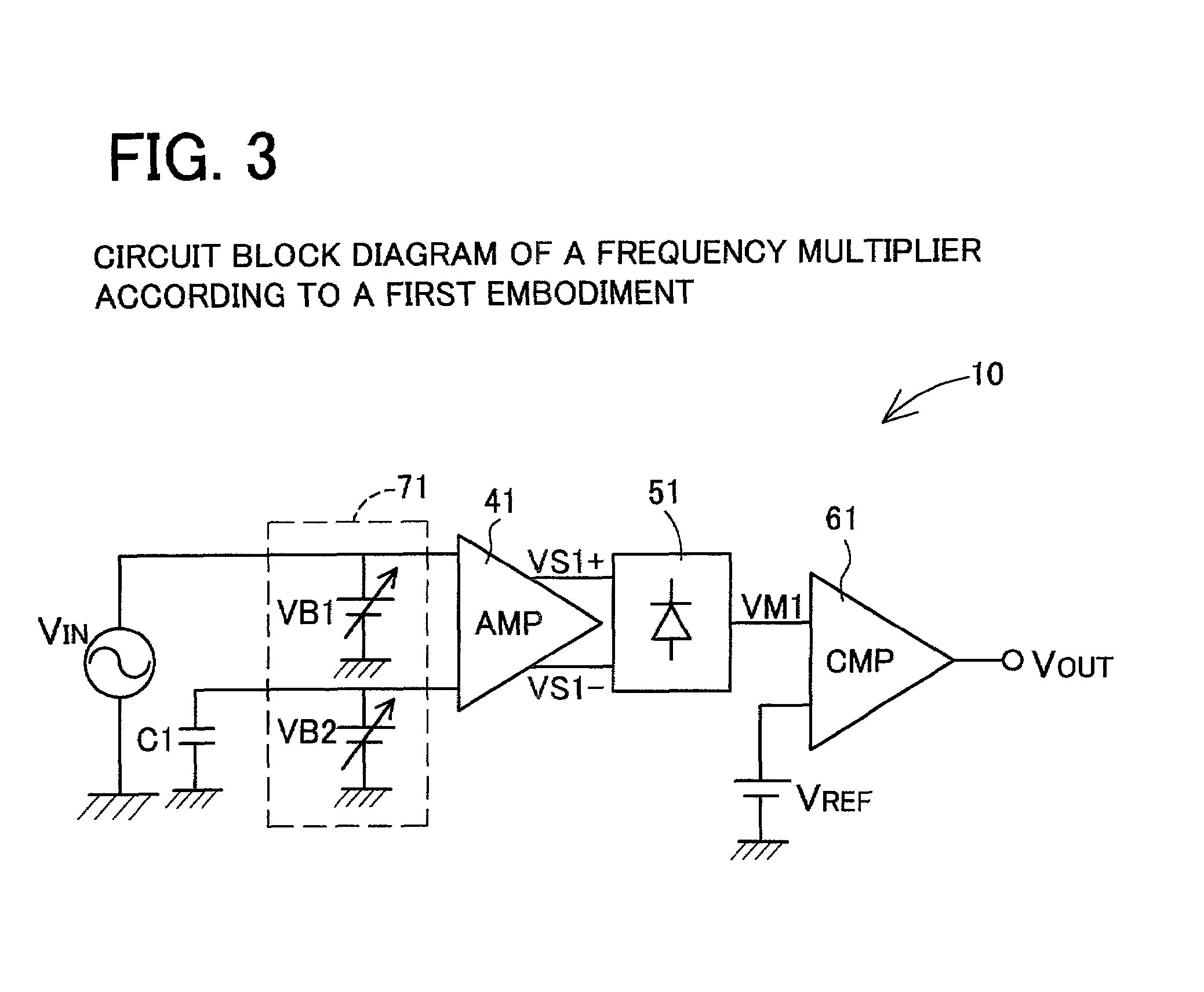
[0050]The first embodiment is directed to the case that the input frequency signal VIN is input to the one differential input terminal of the differential amplifier 41 as a single-phase signal. However, the invention is not limited to such a case; for example, input frequency signals VIN as differential signals may be input to the differential amplifier 41. In the latter case, the capacitance C1 (grounding capacitance) that is connected to the other differential input terminal is not necessary.

[0051]FIG. 4 shows input-output response waveforms in a case that a sinusoidal waveform such as a sine wave is input as an input frequency signal VIN. In the case of FIG. 4, the bias voltage values of the voltage sources VB1 and VB2 are set at the same voltage. Differential output signals VS1+ and VS1− of the differential amplifier 41 have opposite phases. A full-wave-rectified signal VM1 produced by the full-wave rectifier 51 from the differential output signals VS1+ and VS1− has such a wavef...

second embodiment

[0114]In the second embodiment, the frequency of an output frequency signal VOUT is switched among the same frequency as the frequency of an input frequency signal VIN and its double, triple, and quadruple frequencies by generating four-phase signals that are deviated from each other in phase by 90° based on the input frequency signal VIN. However, the invention is not limited to such a case. An output frequency signal VOUT whose frequency is an arbitrary multiplication number of times higher than the frequency of an input frequency signal VIN can be obtained by generating multi-phase frequency signals having arbitrary phase differences. For example, an output frequency signal VOUT whose maximum frequency is six times higher than the frequency of an input frequency signal VIN can be obtained by generating six-phase frequency signals that are deviated from each other in phase by 60°.

[0115]The first to third embodiments are directed to the case that a sinusoidal signal such as a sine ...

fourth embodiment

[0116]In the fourth embodiment, a signal having a prescribed voltage value is input as an input frequency signal VIN. However, the invention is not limited to such a case. A modification is possible in which a current signal, rather than a voltage signal, is input and a current / voltage converter is disposed preceding stage of the V / F converter 82 or a current / frequency converter is provided instead of the V / F converter 82.

[0117]The first and second embodiments are directed to the case that the reference voltage VREF of the comparators 61, 61A, and 62 is a fixed value. However, the invention is not limited to such a case. It is also possible to change the multiplication number of the frequency of an output frequency signal VOUT by adjusting the reference voltage VREF as appropriate. For example, in the frequency multiplier 20 according to the second embodiment, if the bias voltage value of the voltage source VB23 is higher than that of the other voltage sources VB21, VB22, and VB24 (...


PUM


Abstract

It is intended to provide a frequency multiplier capable of switching as appropriate among frequency signals having frequencies obtained by multiplying prescribed multiplication numbers with low current consumption and a simple circuit configuration in effectively utilizing frequencies in radio communication equipment. The base terminals of an input differential pair are biased by respective voltage sources, and an input frequency signal is input to one of the base terminals. The differential output terminals are connected to the base terminals of next-stage buffer circuit transistors, and their emitter terminals are connected to respective diodes. A full-wave-rectified signal, which is obtained at the connecting point of the cathode terminals of the diodes, is input to a comparison differential pair, which produces an output frequency signal by comparing the full-wave-rectified signal with a reference voltage. The frequency of the output frequency signal is switched as appropriate between the same frequency as the frequency of the input frequency signal and its double frequency by the manner of setting the bias voltages of the voltage sources.

Description

BACKGROUND OF THE INVENTION[0001]1. Field of the Invention[0002]The present invention relates to a frequency multiplier. In particular, the invention relates to a frequency multiplier that is used in radio communication equipment and is capable of switching the output frequency.[0003]2. Description of the Related Art[0004]Nowadays, with the number of transmission carrier frequency bands increases for more effective use of frequencies, radio communication equipment such as cellular phones is increasingly used in such a manner that the carrier frequency is switched. Frequency multipliers also need to be used in such a manner that switching is made as appropriate among a plurality of frequencies (multiplication numbers), and are required to be able to switch the frequency easily. On the other hand, there are no bounds to the requirements of multi-functionality and size reduction for equipment. In portable equipment such as cellular phones that are a typical example of radio communicati...

Claims


Application Information

Patent Timeline
IPC IPC(8): H04B1/04H03B19/16H03B19/14
CPCH03B19/14
Inventor ARIMURA, KAZUYOSHI
Owner SOCIONEXT INC
Why Eureka
Try Eureka