
Nanowire electron scattering spectroscopy

a nanowire electron scattering and spectroscopy technology, applied in the direction of optical radiation measurement, instruments, spectrometry/spectrophotometry/monochromators, etc., can solve the problems of inability to realize the full effect of the sensor, inability to realize the sensor, and inability to achieve the effect of reducing the cost of the functionalization step, facilitating the fabrication of the sensor system, and facilitating the electrical readou

Inactive Publication Date: 2009-06-16
CALIFORNIA INST OF TECH
View PDF2 Cites 5 Cited by
  • Summary
  • Abstract
  • Description
  • Claims
  • Application Information

AI Technical Summary

Benefits of technology

NESS allows for single molecule sensitivity and identification of molecular species without labor-intensive functionalization, simplifying sensor fabrication and enabling compact, low-power systems for applications like astrobiology and planetary characterization.

Problems solved by technology

However, the optimization of such sensors is still in its infancy.
Therefore, this additional, costly functionalization step must be done differently for each type of molecule and many differently functionalized nanotubes would be required for detection of a broad range of chemicals.
As a consequence, while potentially effective, this functionalization requires labor-intensive treatment of many nanowires to sense a broad spectrum of molecules.
For both fluorescent and Raman measurements, the optics are typically not integrated on chip, require alignment, and tend to be rather bulky.
Thus, unlike the NESS concept of the present disclosure, the IETS approach does not allow real-time detection of multiple chemical species presented to the sensor after device fabrication.

Method used


Image

  • Nanowire electron scattering spectroscopy
  • Nanowire electron scattering spectroscopy
  • Nanowire electron scattering spectroscopy

Examples


Embodiment Construction

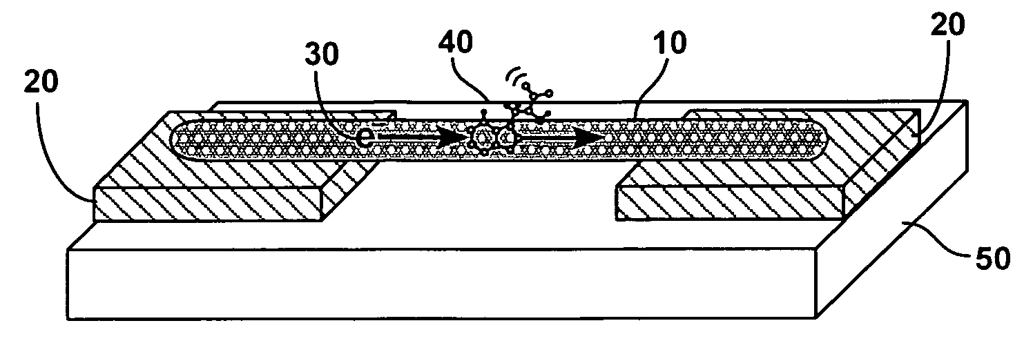
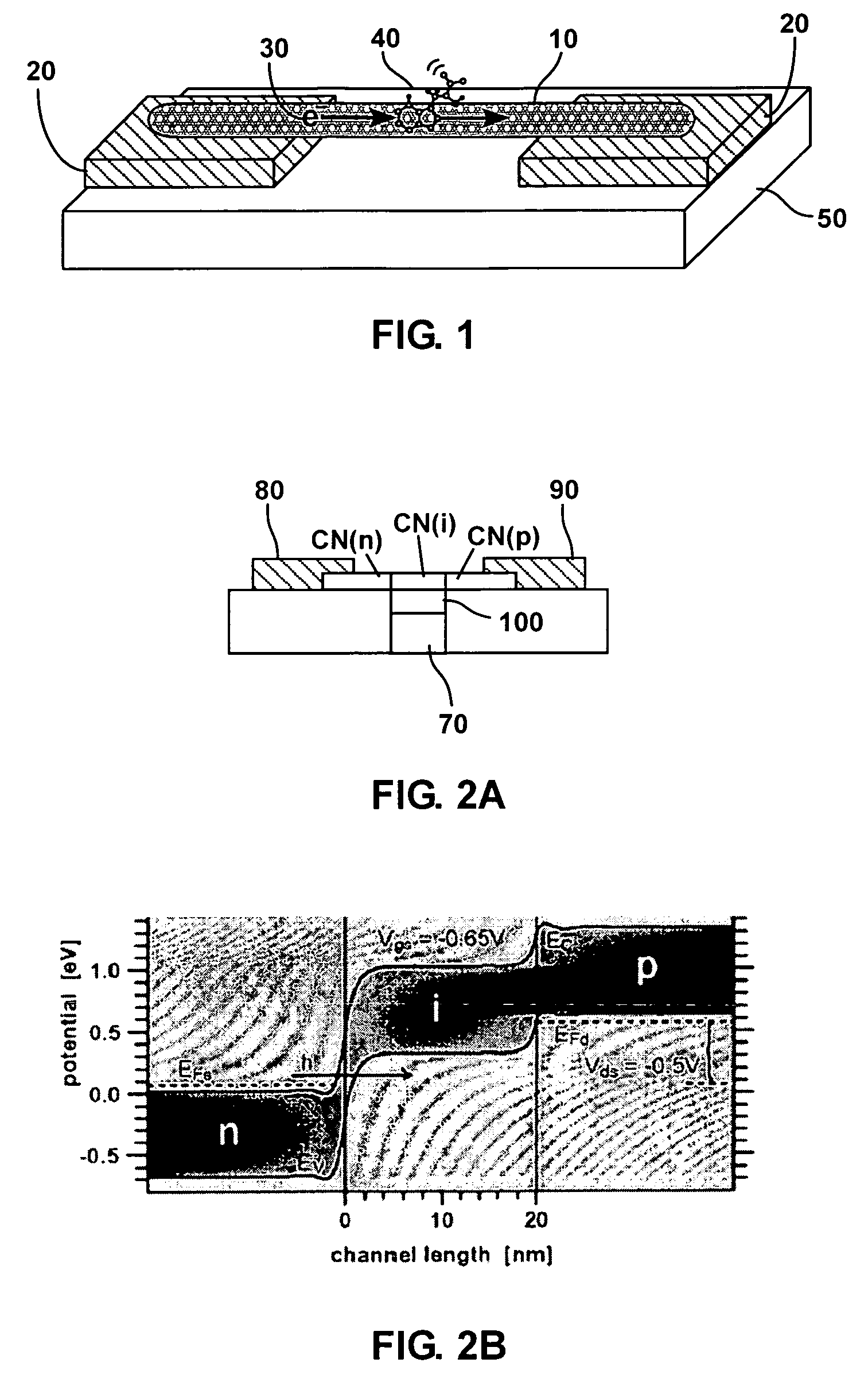
[0026]FIG. 1 is a schematic diagram showing a nanotube or nanoscale wire (nanowire) 10 connected with at least two electrodes 20, thus forming a nanotube suspended bridge. The person skilled in the art will understand that a nanoscale wire has a nanoscale diameter (less than 100 nm), but may have a much longer length on the order of microns or more. The micron scale length enables practical external coupling via electrode contacts in order to monitor the unique electrical properties associated with the nanometer cross-sectional dimensions. Electrons 30 are injected at energies determined by the voltage bias across the nanotube 10. When electron energies correspond to particular molecular vibrational levels in attached molecules 40, enhanced electronic scattering leads to a measurable change in conductance at that voltage. Also shown in the figure is a substrate 50. Typical voltage biases will range from zero to several hundred milli-electron volts (meV) (for example, approximately 0...


PUM

PropertyMeasurementUnit
energyaaaaaaaaaa
diameteraaaaaaaaaa
voltageaaaaaaaaaa

Abstract

Methods and devices for spectroscopic identification of molecules using nanoscale wires are disclosed. According to one of the methods, nanoscale wires are provided, electrons are injected into the nanoscale wire; and inelastic electron scattering is measured via excitation of low-lying vibrational energy levels of molecules bound to the nanoscale wire.

Description

CROSS REFERENCE TO RELATED APPLICATIONS[0001]This application claims the benefit of U.S. provisional Patent Application Ser. No. 60 / 713,827 filed Sep. 2, 2005 for “Nanowire Electron Scattering Spectroscopy” by Brian D. Hunt, Michael Bronikowski, Eric W. Wong, Paul von Allmen and Fabiano A. Oyafuso, the disclosure of which is incorporated herein by reference.STATEMENT REGARDING FEDERALLY SPONSORED RESEARCH OR DEVELOPMENT[0002]The invention described herein was made in the performance of work under a NASA contract, and is subject to the provisions of Public Law 96-517 (35 USC 202) in which the Contractor has elected to retain title.BACKGROUND[0003]1. Field[0004]The present disclosure relates to methods and devices for sensing. In particular, it relates to devices and methods for nanowire electron scattering spectroscopy.[0005]2. Related Art[0006]Optical fluorescence techniques are capable of single molecule sensitivity and are well suited to surveying relatively large volumes. However...

Claims


Application Information

Patent Timeline
Patent Type & Authority Patents(United States)
IPC IPC(8): G01N27/12
CPCB82Y15/00G01N23/221
Inventor HUNT, BRIAN D.BRONIKOWSKI, MICHAELWONG, ERIC W.VON ALLMEN, PAULOYAFUSO, FABIANO A.
Owner CALIFORNIA INST OF TECH
Learn More