

Method and system for performing crosstalk analysis
a crosstalk analysis and analysis method technology, applied in the field of methods, can solve the problems of victim wire switching too slowly, victim wire switching too quickly, and the intended operation of the ic to fail
- Summary
- Abstract
- Description
- Claims
- Application Information
AI Technical Summary
Benefits of technology
Problems solved by technology
Method used
Image

Examples
Embodiment Construction
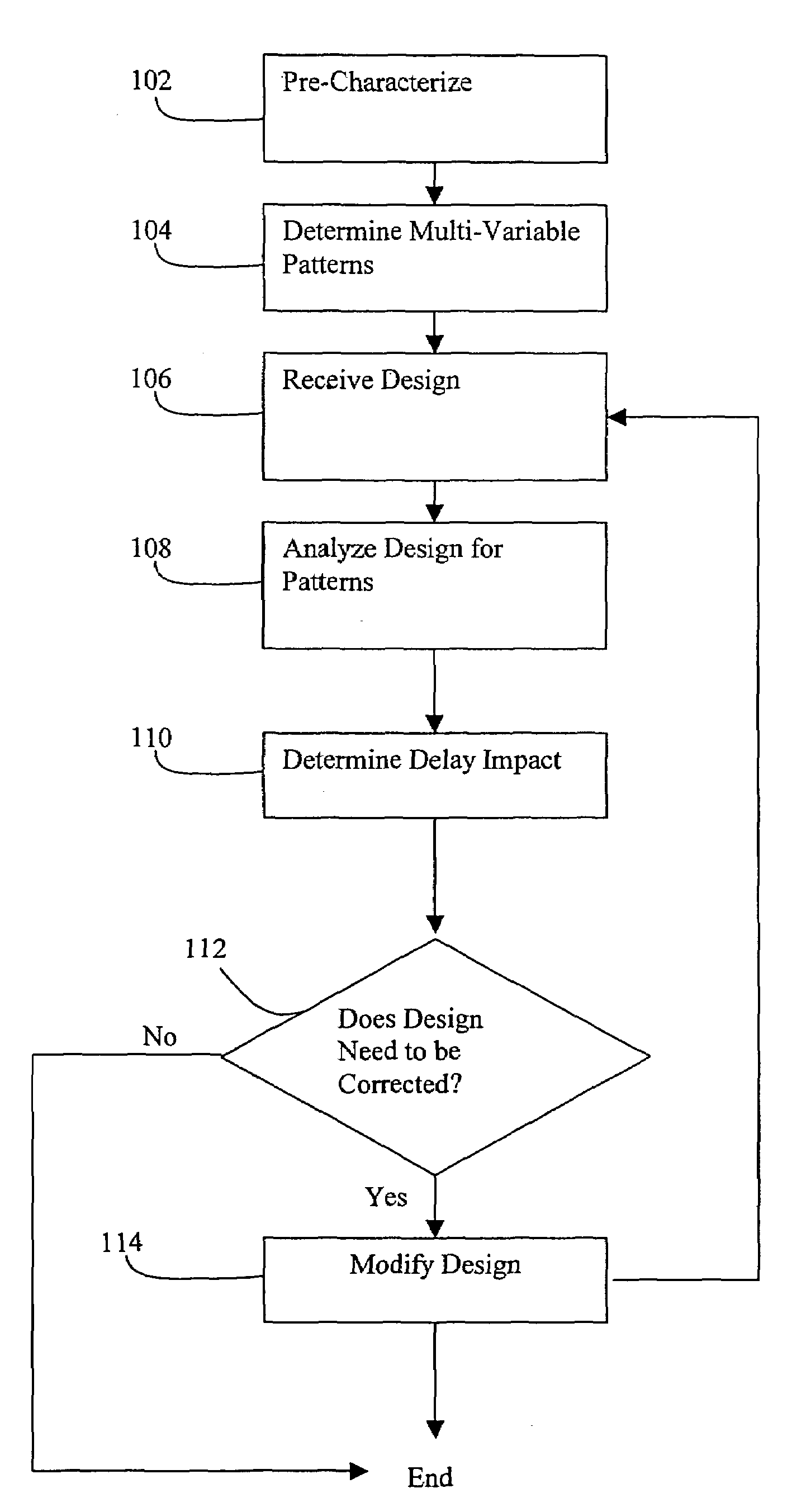
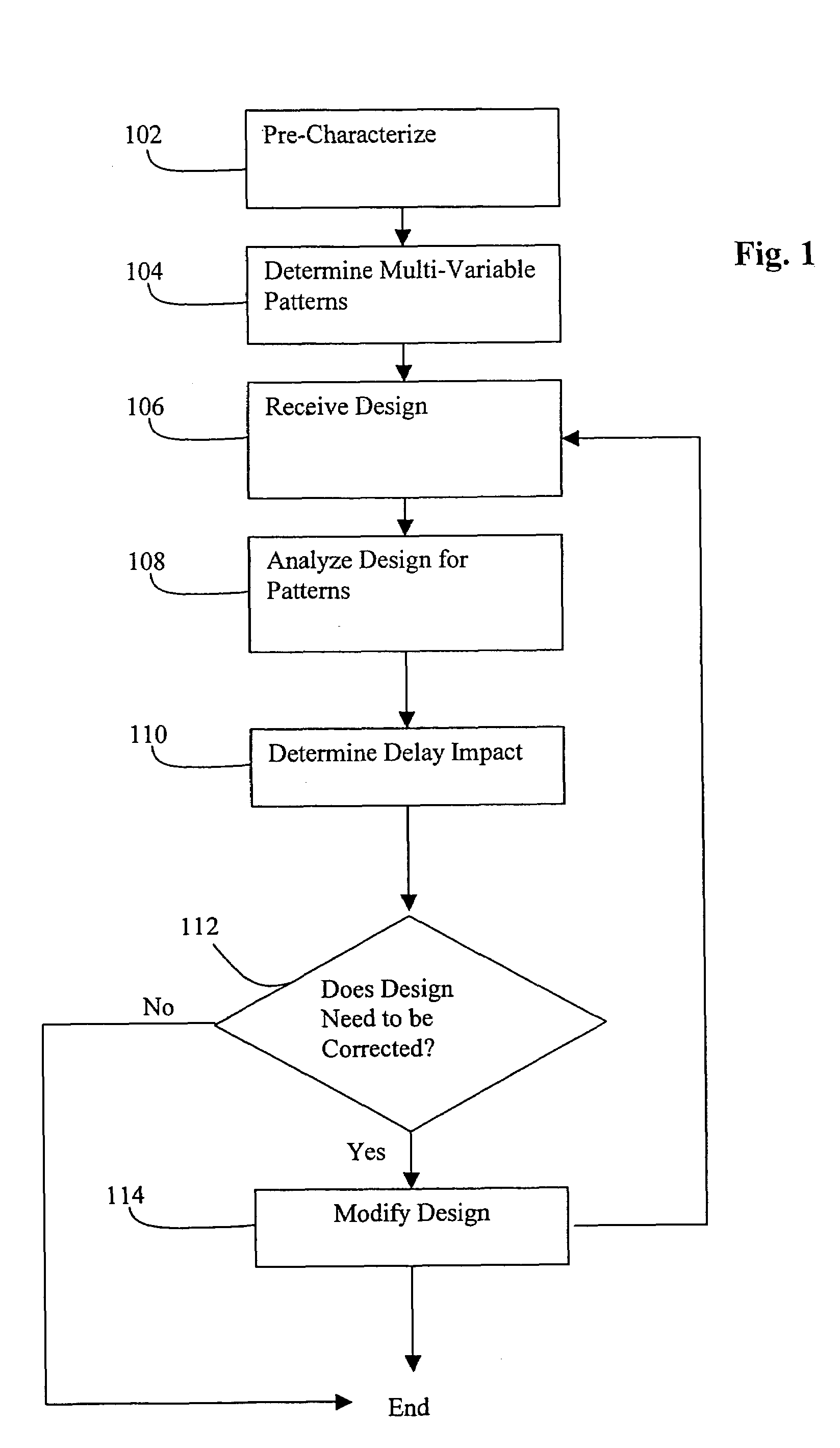
[0018]The present invention is directed to a method and mechanism for performing crosstalk and signal integrity analysis. In an embodiment, multi-variable pattern analysis is performed to implement the crosstalk analysis. Generally, this approach is performed by determining a set of multi-variable patterns corresponding to characteristics related to crosstalk effects. Each of these patterns can be analyzed and associated with a delay impact. Once an IC design is ready to be analyzed, the design is reviewed to determine whether any of the pre-characterized patterns are identified. The delay impact can therefore be readily determined from identifying these patterns.
[0019]FIG. 1 shows a flowchart of a process for crosstalk analysis according to an embodiment of the invention. At 102, device-level pre-characterization is performed. This action can be accomplished by performing device-level simulations / modeling that are run by systematically modifying the value of variables that are to b...
PUM
 Abstract
Description
Claims
Application Information