Scanning imager employing multiple chips with staggered pixels

a scanning imager and image capture technology, applied in the field of solid state imagers and image capture systems, can solve the problems of ccd imagers, speed limitations, and size limitations

Inactive Publication Date: 2009-06-30
DYNAMAX IMAGING
View PDF4 Cites 53 Cited by
  • Summary
  • Abstract
  • Description
  • Claims
  • Application Information

AI Technical Summary

Benefits of technology

[0008]Accordingly, it is an object of the present invention to provide a solid-state imager that can be employed in a scanning system and that avoids the drawbacks of the prior art.
[0009]It is another object to provide an imager that is economical and effective over a width sufficient for scanning a text document.
[0010]It is another object to improve the effective resolution of a monochrome or color imager.

Problems solved by technology

This size limitation arises because of charge transfer difficulties over large distances, i.e., over distances comparable to the width of a page.
While it might be desirable to join a number of CCD imagers end to end to create in effect a single long image capture device, there are many drawbacks that make that impractical.
The CCD imagers have many drawbacks and limitations, such as speed limitations, which arise due to charge transfer efficiency limitations, as well as a high power consumption, and a severely limited capability for integration of other functions onto the pixel array.
In addition, in CCD imagers the pixels must be read out in a fixed sequence, which does not permit pixel information to be skipped.
Accurate placement of the CIS modules 32(1)-32(N), which is necessary to pick up the entire image without gaps or jumps across the width of the object, makes the construction of the CIS-based system rather expensive.
Also, the various individual CIS sensors each have individual voltage offsets that have to be corrected, and this also adds to the complexity of the system.

Method used


Image

  • Scanning imager employing multiple chips with staggered pixels
  • Scanning imager employing multiple chips with staggered pixels
  • Scanning imager employing multiple chips with staggered pixels

Examples


Embodiment Construction

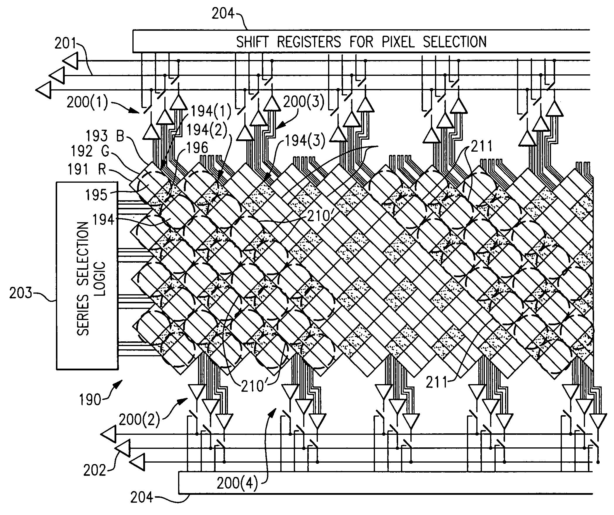
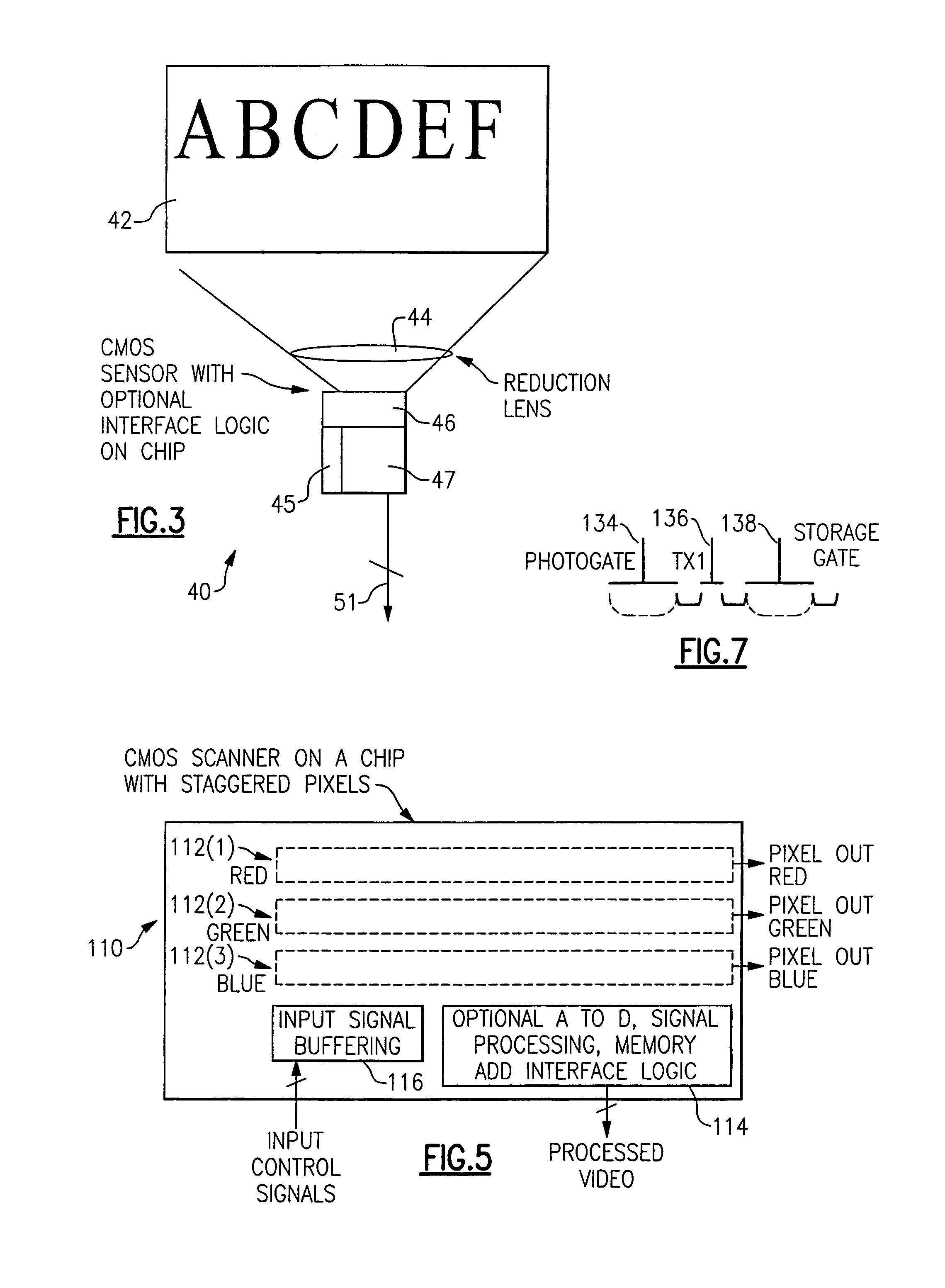
[0036]With reference now to the Drawing, and initially to FIG. 4 thereof, a system 40 for capturing an image of an object 42, e.g., text, in accordance with an embodiment of the invention includes a lens 44, a CMOS imaging system 46, an image control processing system 47, and an output bus 51. Other equivalent components could be used. The image control processing system 47 may be included on the CMOS sensor 46 to eliminate need for a separate component and reduce overall cost. The present invention provides a system for capturing an image with greater flexibility and lower cost than prior systems that use CCD or CIS technology. Additionally, the present invention provides a unique offset pixel structure for use in the CMOS imaging system 46.

[0037]As shown in FIG. 3, the lens 44 is positioned in the system to focus or direct the image being scanned or otherwise captured onto the CMOS imaging system 46. In this embodiment, the lens 44 reduces the image being scanned onto the CMOS ima...


PUM


Abstract

A solid state imaging system has at least one CMOS imager with first and second series of pixels in which the pixels of one series are offset, i.e., staggered, in respect to the pixels of the other series. Multiple imagers can be arrayed end to end, with jumper wires connecting the pixel output conductors or each so that the pixels feed into a common output amplifier for each series, to minimize chip to chip offset voltages. The pixels may be diagonally offset from one another, and a color imager can be constructed in which color ribbon filters are arranged diagonally across the imaging area. This arrangement minimizes color cross talk. An array of microlenses is situated with each microlens covering a plurality of the pixels. The different pixels under each microlens can be aligned along a diagonal. The different pixels under the same microlens can have different integration times, to increase the dynamic range of the imager(s).

Description

CONTINUING APPLICATION DATA[0001]This is Continuation-in-Part of application Ser. No. 11 / 434,666, filed May 16, 2006, now U.S. Pat. No. 7,129,461, which is a a division of Ser. No. 11 / 356,199, Feb. 17, 2006, now U.S. Pat. No. 7,122,778, which is a division of Ser. No. 11 / 111,334, Apr. 21, 2005, now U.S. Pat. No. 7,045,758, May 16, 2006, which is a continuation in part of earlier patent application Ser. No. 10,141,008, May 7, 2002, now U.S. Pat. No. 6,911,639, which claims priority of U.S. Provisional Application No. 60 / 289,076, May 7, 2001, now abandoned. The foregoing are incorporated herein by reference.BACKGROUND OF THE INVENTION[0002]This invention concerns solid state imagers and image capture systems, and in particular is directed to an improved configuration of the pixels into offset or staggered arrangements of two or more series of pixels. The invention is more particularly concerned with a configuration that allows two or more imager chips to be butted end-to-end, and whic...

Claims


Application Information

Patent Timeline
Patent Type & Authority Patents(United States)
IPC IPC(8): H01L27/00H04N3/14
CPCH01L27/14603H01L27/14621H01L27/14627H04N1/1911H04N1/1917H04N3/1581H04N5/2254H04N9/045H04N2201/0081H04N25/701H04N25/778H01L27/146H04N25/57H04N25/76
Inventor ZARNOWSKI, JEFFREY J.KARIA, KETAN V.JOYNER, MICHAELPOONNEN, THOMASLIU, LI
Owner DYNAMAX IMAGING
Why Eureka
Try Eureka